ChillOne: one circuit board of our own
What changed (4 Nov 2026). The rev A design of the smart door frame is built from bought boards joined by leads: a Raspberry Pi Zero 2 W, a Camera Module 3 Wide, an Adafruit MLX90640 heat-camera board, an LD2410C radar module, an SHT45 board, a DS18B20 probe, a Walter LTE-M board, an ATECC608 board, two NeoPixel sticks, a PowerBoost 1000C, a Waveshare e-paper board and a reed switch in the strike jamb. ChillOne now gets one circuit board of our own, like CricketOne and CellOne, with every chip soldered straight on it:
- The chips: the V1 brain (Rockchip RV1126B, memory, eMMC, latched microSD, certified Wi-Fi/Bluetooth module), the C1 colour camera chip (Sony IMX335), an Infineon 60 GHz radar chip, a bare Melexis heat-camera chip, a Quectel LTE-M modem with a soldered eSIM, a TI ±0.1 °C probe chip, a Sensirion air chip, a TI 3D Hall chip for the door, the security chip, sixteen call-light LEDs, a sounder, the e-paper panel, a certified Mean Well mains module and a backup cell with its charger.
- The shape: one rigid-flex board in the frame’s own tube. A rigid 8-layer head (420 × 82 mm) stands upright in the header, 17 mm behind the inside face. A camera tab in a U-slot of the head folds 35° out, so the camera and radar look down into the room. A door tip on a 6 mm flex lies on the header floor over the door, a probe finger reaches into the glycol vial, and a 24 mm flex tail runs along the header, down through a slot into the hinge jamb, and S-bends to a rigid 4-layer panel (80 × 160 mm) at eye height behind the display.
- No strike-jamb part and no wire across the door. The reed switch and its magnet are replaced by a 3D Hall chip on the door tip over a magnet in the door’s top edge: it reads door shut and how far it stands ajar.
- Mains stays in the hinge jamb. The frame already carries 120 V for its heater wire and light; the panel takes it on a push-in terminal into a fused, certified IRM-05-5 module, at least 6.4 mm from every low-voltage part. Only low voltage goes up the tail.
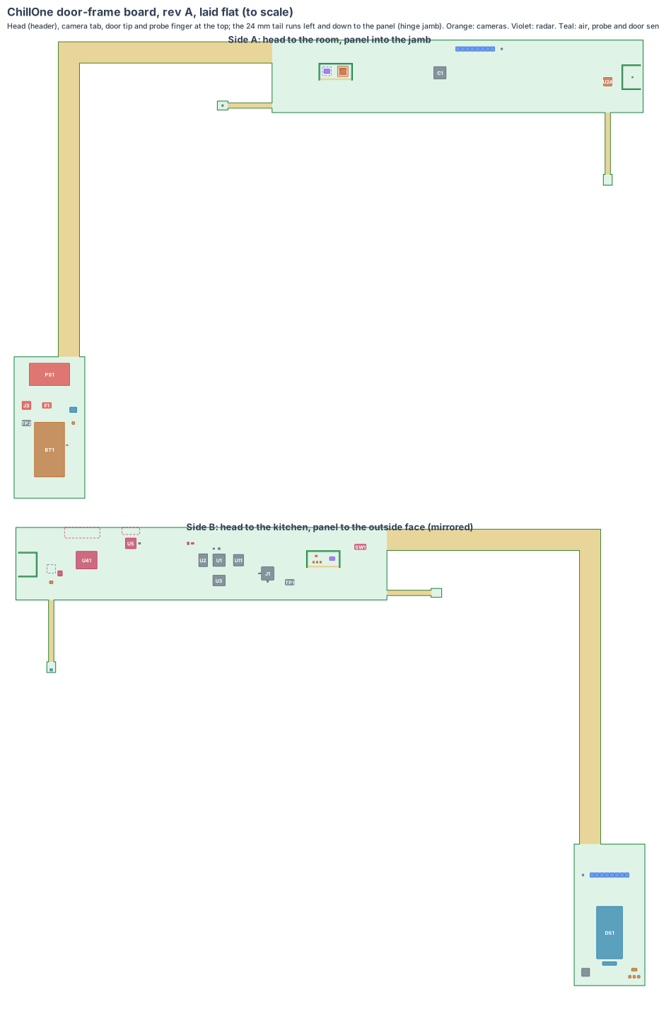
The board is code (hardware/pcb/chillone-board.mjs). It writes the KiCad board file (chillone-board.kicad_pcb), the parts list (chillone-board-parts.csv) and this drawing, and checks every part:
- every part sits on its section with a 0.3 mm edge margin, clear of both U-slots and every flex, and no two parts overlap on the same side;
- every part’s height fits its gap: 17 mm on the head’s room side, 77 mm on its kitchen side, 2.3 mm on the panel’s outside face, 91.7 mm inside the jamb;
- the head sits inside the header cavity, the panel inside the hinge jamb, and the tail passes the new slot in the header floor;
- the heat-camera can, both rows of call-light LEDs, the air chip at the vents, the e-paper, and the sounder under its tone holes each sit on their window in the frame CAD (within 1 mm);
- folded, the camera tab looks 35° down like the CAD’s room view, its axis meets the camera window’s centre (0.0 mm off), and the lens holder stays 1.25 mm clear of the inside face;
- the heat-camera can comes forward on a 10 mm lead spacer to 0.4 mm behind the face, so its 110° view needs only a 9.7 mm opening in the Ø14 window;
- the door tip ends 2.4 mm clear of the outside wall and puts the Hall chip 10.9 mm from the door magnet (about 14 mT, est.);
- the probe tip lies inside the Ø16 glycol vial on its axis;
- mains creepage: every non-mains part is 6.4 mm or more from the terminal and fuse;
- the Wi-Fi and LTE-M antenna keep-outs are at the head’s top edge, 25 mm apart; the air chip is 56 mm or more from every warm part.
KiCad design rule check: 0 violations, 0 unconnected items (KiCad 10, 4 Nov 2026). Each part is drawn at its real size, as a placeholder outline until its full footprint is added.
Sizes come from the frame CAD (cad/chillone-cad.mjs, rev A: 100 mm face, 101.6 mm deep FRP tube with 3 mm walls round a 864 × 1930 mm opening) and the chip datasheets. Numbers marked est. are estimates.
1. The board and where each part sits
| Section | Size | Where | Build |
|---|---|---|---|
| Head | 420 × 82 mm | upright in the header, x −230 to 190, z 1940 to 2022; side A (room) 17 mm behind the inside face | rigid, 8 layers, 1.6 mm |
| Camera tab | 36 × 16 mm | in a U-slot of the head at x −176 to −140, hinged 38.75 mm above the head’s bottom edge, folded 35° out | rigid, 4 layers, 0.8 mm, on a 2 mm flex hinge |
| Door tip | 10 × 12 mm | on a 6 × 70 mm flex from the head’s bottom edge at x 150: down 6 mm, then across the header floor to 2.4 mm from the outside wall | stiffened 2-layer flex, bonded to the floor |
| Probe tip | 12 × 10 mm | on a 6 × 50 mm flex from the head’s −x edge, inside the glycol vial at x −296 to −266 | stiffened 2-layer flex, potted |
| Tail | 24 mm wide, 344 mm folded | along the header, down through a slot in the header floor at x −473 to −447, S-bent across the jamb to the outside face | 2-layer flex |
| Panel | 80 × 160 mm | in the hinge jamb, x −522 to −442, z 1540 to 1700; side B 2.3 mm behind the outside face | rigid, 4 layers, 1.6 mm |
Why this shape: the frame is a hollow tube all the way round the door, and its windows sit along the header’s inside face and the hinge jamb’s outside face. One upright board in the header reaches the room windows; the display, the mains feed and the cell belong at eye height in the hinge jamb, the side that does not swing. Flex reaches the rest instead of cables.
Changes to the frame CAD (rev B; nothing is bought for them):
- Camera window Ø12 → Ø26 clear PC. The camera now sits on a folded tab 7.7 mm behind the face; its 105° view needs 24.5 mm.
- Air vents move from x 400 to x 178, over the air chip’s tongue.
- Outside call-light slot and the tone holes move to the hinge jamb (z 1665 and z 1555), beside the display.
- A 26 × 4 slot in the header floor at x −473 to −447 for the tail; the old tamper hole at x −482 is filled.
- The header’s outside face becomes a screwed service cover with a rib that presses the tamper switch; the microSD card is reached behind it.
- The glycol vial becomes Ø16 × 30 lying along the header at x −296 to −266, with a seal round the probe finger.
- A Ø6 × 3 N52 magnet in the door leaf’s top edge at x 150 (the strike-jamb reed switch and its magnet are removed).
2. What is on the board
The V1 brain core (copied from CricketOne’s brain section) and the C1 colour camera chip (as CellOne), in ChillOne’s shape. Only what is different for a walk-in is described after the table.
| Ref | Part | Size (mm) | Section, side |
|---|---|---|---|
| U1 | Rockchip RV1126B, thermal pad to a 50 × 40 × 2 aluminium spreader | 14 × 14 | head, kitchen |
| U2, U11 | LPDDR4X 1 GB; eMMC 5.1 8 GB industrial | 10 × 14.5; 11.5 × 13 | head, kitchen |
| U3, Y1, Y2 | RV1126B power rails; 24 MHz and 32.768 kHz MEMS oscillators | zone; 2.5 × 2; 2 × 1.6 | head, kitchen |
| J1 | microSD socket, hinged and latched, fitted on every board: our software starts from the card | 14 × 15 | head, kitchen |
| U5, ANT1 | AMPAK AP6256 Wi-Fi 5 + Bluetooth 5 (certified), chip antenna at the top edge | 12 × 12 × 1.65 | head, kitchen |
| U41, U42, ANT2 | Quectel BG95-M3 LTE-M modem, MFF2 eSIM soldered, LTE antenna at the top edge | 23.6 × 19.9 × 2.2 | head, kitchen |
| U8, U9 | Microchip ATECC608B security chip; ID EEPROM | 2 × 3 | head, kitchen |
| SW1 | Omron D2F-01 tamper switch, pressed by the service cover’s rib | 12.8 × 5.8 × 6.5 | head, kitchen |
| U24, U25 | Melexis MLX90640ESF-BAA heat-camera chip (32 × 24, 110 × 75°), TO-39 can on a 10 mm lead spacer at the heat window; its LDO | Ø9.6 × 16.6 with spacer | head, room |
| U10 | Sensirion SHT45 air chip on a slotted tongue at the vents | 1.5 × 1.5 | head, room |
| D1–D8, U36 | inside call light: 8 RGB LEDs (WS2812B class) behind the opal slot; level shifter | 5 × 5 × 1.6 | head, room |
| U20, LH1 | Sony IMX335 5 MP colour camera chip under an M8 holder with a 2.1 mm wide lens (about 105°, est.) | 7.3 × 7.1; 12 × 12 × 10 | camera tab, room |
| U26 | Infineon BGT60TR13C 60 GHz radar, antennas in the package, with a 10 × 10 keep-out | 6.5 × 5 × 0.9 | camera tab, room |
| U21–U23, Y20, U27 | camera LDOs and MEMS oscillator; radar LDOs and oscillator | zones | camera tab, back |
| U15 | TI TMAG5273 3D Hall chip: door shut and how far it stands ajar | 2.9 × 2.8 × 1.1 | door tip |
| U14 | TI TMP117 ±0.1 °C chip, potted in the glycol vial: the food and vaccine probe | 2 × 2 × 0.8 | probe tip |
| DS1, PD1, U33 | 2.13 in e-paper panel (now, min, max) on foam tape at the window; its tail hot-bar soldered; booster | 29.2 × 59.2 × 1.2 | panel, outside / inside |
| D9–D16, U37 | outside call light behind the new jamb slot; level shifter | 5 × 5 × 1.6 | panel, outside |
| LS1 | low-profile SMD piezo sounder under the tone holes | 9 × 9 × 1.9 (est.) | panel, outside |
| J3, F1, PS1 | push-in mains terminal (2 poles, 5 mm); fuse and MOV; Mean Well IRM-05-5 5 V 5 W certified module, soldered | 10 × 9; 10 × 6; 45.7 × 25.4 × 21.5 | panel, inside |
| BT1, RT1 | 1,200 mAh Li-ion polymer backup cell in a printed clip, leads soldered; NTC thermistor on the pack | 34 × 62 × 5.5 | panel, inside |
| U30–U32, RS1, U34 | TI BQ24074 charger with power path; protection; gauge; current sense; TI TPS61023 5 V boost for the LEDs in a power cut | 3 × 3 each | panel |
| TP1, TP2 | factory pads (USB, serial, boot, rails; cell, charger, isolated mains test points) | 10 × 6 | head, panel |
What is different for a walk-in:
- The camera and the radar look down from a folded tab. The room view is 35° down (the CAD’s checked view). A camera chip flat on an upright board would look level, so the tab carries the camera and the radar chip and folds out on a 2 mm flex hinge. The radar keeps the person-still-inside call working with the lights off.
- A buffered probe of our own. The DS18B20 on a cable becomes a TMP117 on a flex finger potted in the glycol vial: ±0.1 °C without calibration, read over I2C. It answers the vaccine data-logger rule’s buffered probe and the food code’s thermometer.
- LTE-M on the board. The Walter board becomes a BG95-M3 modem with a soldered eSIM, so the power-loss alarm still goes out by SMS when the site’s power and Wi-Fi are down.
- Power cuts. The cell keeps the RV1126B asleep between 5-minute signed readings, with the modem in its power-saving mode (about 0.08 W average, about 40 h, est.). The TPS61023 lights the call LEDs from the cell.
- No mains in the header. Mains comes up the hinge jamb as it does today for the heater wire and light, and stops at the panel.
Sale boards boot from the card; the eMMC ships empty, so the card always starts first (Rockchip tries the eMMC before the card), updates write two system copies (a bad update rolls back by itself) and never run during a call or a power cut.
3. Every connection, checked
Our rule: every pair of parts that join is checked against both makers’ drawings and a search for known problems. No “same as CellOne” claims.
| Joint | Type | Keyed | Locked | Check |
|---|---|---|---|---|
| Mains feed ↔ panel | push-in PCB terminal, 2 poles, 5.0 mm pitch | pole marks | spring clamp | to check: the exact terminal (Phoenix or Würth) for 120 V and the frame’s wire size (AWG 18–14), its creepage from the maker’s drawing, and the feed’s own fuse in the walk-in’s panel |
| Mains module ↔ panel | IRM-05-5 pins through the panel, soldered | the module’s pin layout | soldered | Mean Well IRM-05 drawing: pin pitch and the isolation slot under it |
| E-paper ↔ panel | the panel’s own FPC tail, hot-bar soldered to pads | pin 1 mark | soldered | to check: the Good Display GDEY0213B74 FPC pitch and pad layout, and its booster circuit, from the maker’s drawing; the panel bonded with foam tape, no connector |
| Backup cell ↔ panel | the cell’s leads soldered to pads, thermistor on the pack | polarity marks on the silkscreen | soldered, cell in a printed clip | the cell maker’s lead and protection notes; no JST plug (the Adafruit-style plug is known to be wired both ways by different sellers) |
| Camera chip ↔ tab | IMX335 CSP BGA soldered on the tab, lens holder screwed | outline | soldered, holder 2 screws | Sony drawing (still to get); the M8 holder’s screw holes from its maker; the MIPI pair over the hinge flex |
| Heat camera ↔ head | TO-39 leads through the board on a 10 mm nylon spacer, soldered | the can’s tab | soldered | Melexis land pattern and lead pitch; to check: a spacer part number and the leads’ length (est. 12.7 mm standard leads) |
| Tabs, tips, tail ↔ head | flex, part of the board | built in | built in | no connectors. To check: the maker’s minimum static bend radius for the tail’s S-bend and the camera hinge (35°) |
| Radios ↔ head | AP6256 and BG95-M3 soldered (LGA, LCC); eSIM soldered | outlines | soldered | AMPAK and Quectel footprints and antenna keep-outs from their hardware guides |
| microSD ↔ head | hinged, latched socket | the socket’s card key | hinged lid latches | Amphenol 101-00660 family drawing |
No adapters, no plug-in modules and no ribbons inside.
4. Heat
- The RV1126B runs about 1.5 W at its busiest (est.); its thermal pad goes to a 50 × 40 × 2 aluminium spreader in the header air. With the header at a 40 °C kitchen’s temperature that is about 63 °C, well under its 85 °C rating (est., checked on rev A).
- The bigger problem is reading the room, not cooling. The air chip sits on its own slotted tongue at the vents, 56 mm or more from every warm part, and the probe chip is buffered in glycol in its vial, out of the board’s warmth.
- Freezers. A freezer door’s header air sits near −5 °C (est.) behind a −25 °C face. The frame’s own heater wire keeps it above the dew point; memory, eMMC and the modem are industrial grade, and the RV1126B’s grade is checked on a freezer door (design review).
- The cell sits in the hinge jamb on the kitchen side, away from the supply (10 mm or more); the thermistor holds charging outside 0–45 °C.
5. Power budget (est.)
| Value | |
|---|---|
| Supply | the frame’s 120 V heater and light feed, through a fused IRM-05-5 (5 W) on the panel |
| Watching (camera frame every 10 s, heat camera 1 Hz, radar, probe, Wi-Fi) | 1.6 W |
| A call (call light, tone, LTE-M send) | 3.0 W, 3.5 W peak |
| Power cut (asleep, a signed reading and an LTE-M check every 5 min) | about 0.08 W average: about 40 h on a 1,200 mAh cell aged to 80 % |
The peak is 70 % of the supply. The first rev A frames on a real walk-in replace these estimates.
6. Factory test (every board, every time)
- Current-limited first power-on from a low-voltage bench supply on the system rail, then from 120 V through an isolating transformer.
- Every rail within ±3 %; the mains side’s insulation tested at the module’s rated voltage.
- Our microSD card in, then boot: the Rockchip SDK image to a shell; eMMC written; the ID chip written; the security chip given its key.
- Camera: a test chart through a fixture window at 35°. Heat camera: a warm and a cold plate. Radar: a moving plate at 1 m and 2 m. Probe: in a 0 °C and a 25 °C bath. Air chip: the fixture’s two chambers. Door chip: a magnet moved from shut to 10° open. Each LED colour read by a light sensor; the sounder’s level; the e-paper drawn and read by a camera.
- Battery: charges from the 5 V rail; protection cuts off at low voltage and on a short; the gauge reads; the thermistor reads. Mains removed: the board stays up on the cell and sends a test SMS.
- Wi-Fi to the fixture; the modem attaches to a test cell. Every result is stored against the serial number.
For each rev A batch: radio pre-scan (FCC Part 15, the 60 GHz radar rule, the modem’s carrier approvals), a 24-hour soak in a cold, wet chamber, and the frame’s electrical safety pre-checks (the frame is to be listed with the walk-in, UL 471 path).
7. Who makes what
| Work | Who |
|---|---|
| Board shape, parts, placement, checks, KiCad files, schematics | IEMI Labs |
| The V1 brain core and C1 colour camera chip | copied from CricketOne’s and CellOne’s boards |
| The board (8-layer head, 4-layer panel and tab, 2-layer flex tail, tips) | a maker that builds rigid-flex boards (see the makers list on the boards page) |
| Assembly, X-ray of the ball-grid chips, the through-board mains module and heat-camera can | the same maker or a Shenzhen assembly house |
| Software: the cold room program on the RV1126B, the IMX335 and radar drivers, the TMP117 probe log | IEMI Labs, on the RV1126B dev kit while the board is made |
8. Cost per frame, electronics (est.)
| qty 10 (rev A) | qty 1,000 | qty 10,000 | |
|---|---|---|---|
| Chips and parts (RV1126B core, IMX335, heat-camera chip, radar, LTE-M + eSIM, mains module, cell, e-paper) | $210–270 | $125–150 | $100–120 |
| Board (rigid-flex: 8-layer head, long 2-layer tail, 4-layer panel) | $70–100 | $14–20 | $10–14 |
| Assembly | $25–40 | $5–8 | $3–5 |
| Per frame | $305–410 | $144–178 | $113–139 |
The heat-camera chip and the LTE-M modem are the biggest parts (about $45 together at volume, est.). The bought parts for the same jobs are $429 at qty 1 (bom.csv, without the frame tubes).
9. Timeline
| When | Step |
|---|---|
| Nov–Dec 2026 | IMX335, radar, TMP117 and TMAG5273 on their makers’ evaluation boards beside the RV1126B dev kit; the cold room calls re-checked on their data |
| Jan 2027 | ChillOne schematics from the V1 and C1 cores; placement (this drawing) into KiCad; review |
| Feb 2027 | rev A made: 10 boards plus spares; bring-up on our fixture |
| Mar 2027 | rev B (fixes, the seven CAD changes), factory test software, radio pre-scan |
| Apr–May 2027 | pilot walk-ins (a restaurant cooler and freezer, a clinic vaccine room); listing work starts |
10. Still to check
- The Sony IMX335 drawing (here 7.3 × 7.1 from a secondary source) and an M8 holder that fits the 12 × 12 × 10 used here.
- The MLX90640ESF-BAA can’s lead length and a 10 mm lead spacer part.
- The push-in mains terminal, its creepage and the frame’s wire size; the IRM-05-5 isolation slot.
- The flex maker’s minimum bend radius for the tail’s S-bend and the camera hinge.
- The 60 GHz radar through 3 mm of FRP: a still person at the back corner, lights off (design review: prove).
- The RV1126B’s temperature grade on a freezer door, and charging the cell in a cold jamb.
- LTE-M and Wi-Fi range from a steel-skinned walk-in wall (design review: prove).
- The CAD alignment (the folded board in the frame CAD with its rev B changes and clearance pockets), as done for CricketOne rev T.
Sources
- Rockchip RV1126B (Forlinx FET1126Bx-S module data: 3 TOPS NPU, ISP up to 12 MP)
- Sony IMX335 5 MP image sensor
- Melexis MLX90640, 32 × 24 thermal sensor (BAA: 110 × 75°)
- Infineon BGT60TR13C, 60 GHz radar, antennas in package, 6.5 × 5.0 × 0.9
- Quectel BG95-M3 LTE-M / NB-IoT module (23.6 × 19.9 × 2.2)
- TI TMP117 ±0.1 °C digital temperature sensor
- TI TMAG5273 3D Hall-effect sensor
- Sensirion SHT45
- TI BQ24074 charger and TI TPS61023 boost
- Mean Well IRM-05 datasheet (45.7 × 25.4 × 21.5)
- AMPAK AP6256 Wi-Fi 5 + Bluetooth 5 module
- Microchip ATECC608B and Omron D2F datasheet
- Good Display 2.13 in e-paper GDEY0213B74
- CDC vaccine storage and handling toolkit (buffered probe, data logger)
- The frame, its sizes and its calls: ChillOne’s design
- The board platform: our own boards
- The camera short that started our board rule: the first stump, section 9
Design review (4 Nov 2026)
Every board is checked by the same rules (products/_shared/board-rules.mjs), one for each lesson any of our boards has taught us. The full review, with every number and its source, is on the board page: 13 pass, 4 fixed, 10 to prove, 0 fail. It changed this board and the frame:
- The camera window grows from Ø12 to Ø26 (CAD rev B): the camera chip sits on a folded tab 7.7 mm behind the face, and its 105° view needs 24.5 mm.
- A hinged, latched microSD socket (J1) and MEMS oscillators (Y1, Y2, Y20) from the start.
- Conformal coating (condensation each time the door opens; frost on freezer doors) asked for in the quote.
- To prove on the dev kit and rev A: the AI engine time, the power-cut hours, Wi-Fi and LTE-M from a steel wall, the door magnet’s field, the radar through the FRP face, and a cold start on a freezer door.
- Fast lines on a solid ground plane (to prove, lesson: planes, from the CricketOne test-board layout of 4 Nov 2026): RV1126B memory; 1 camera MIPI link (100 Ω pairs); USB (90 Ω); antenna feed (50 Ω, keep-out on every layer); card lines (length-matched, no vias under the socket). Ground on the layer next to the parts (inner layer 1, supply on inner layer 2; the whole bottom of a 2-layer section), one via beside each ground and supply pad and none in pads, no copper or vias in the antenna keep-out on any layer or under the card socket, the impedance lines routed first with a test coupon. The quote asks for it; the routed board’s design rule check proves it.
The request for quote is /build/chillone-quote.
New shared rule (4 Nov 2026, from PumpOne): antennas outside metal boxes. A radio inside a closed metal enclosure now fails the review unless its antenna is outside the metal. This board’s antennas already use the header’s FRP face, between the steel skins, so the check passes and the review names the window (lesson: enclosure).
New shared rule (4 Nov 2026, from the CricketOne test-board circuit): the Wi-Fi module’s own clock. Drawing CricketOne’s circuit pin by pin found that the AP6256 Wi-Fi/Bluetooth module runs from a 37.4 MHz reference clock, which our board notes had as 26 MHz or left out. Every board with an AP6256 is now checked for a 37.4 MHz clock beside it (MEMS where the product takes knocks). On this board the AP6256 had no clock of its own on the board; Y3, a 37.4 MHz MEMS oscillator, now sits next to it on the head board. The review shows it under Radio (lesson: wificlock).