

All 48 parts and where they sit
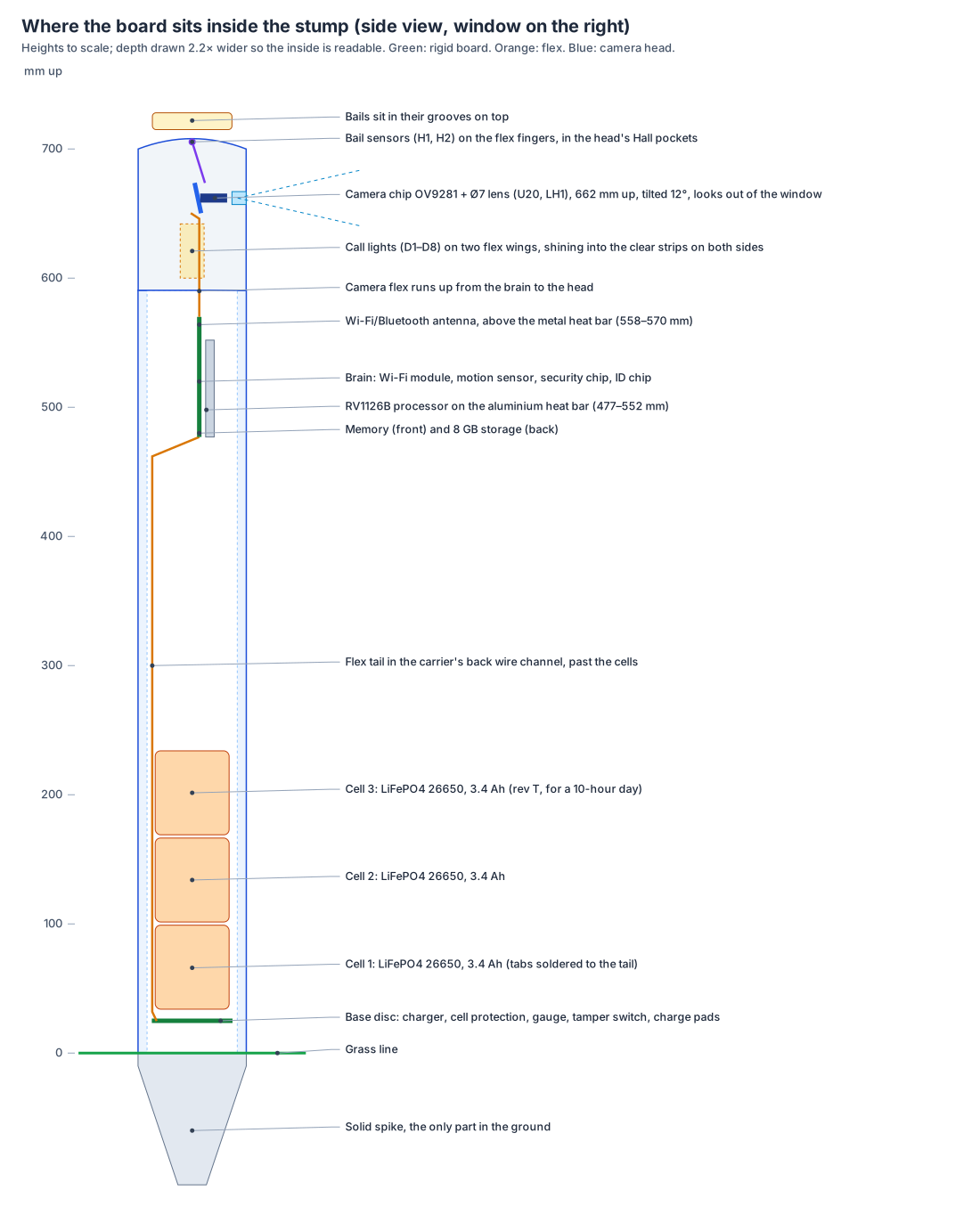
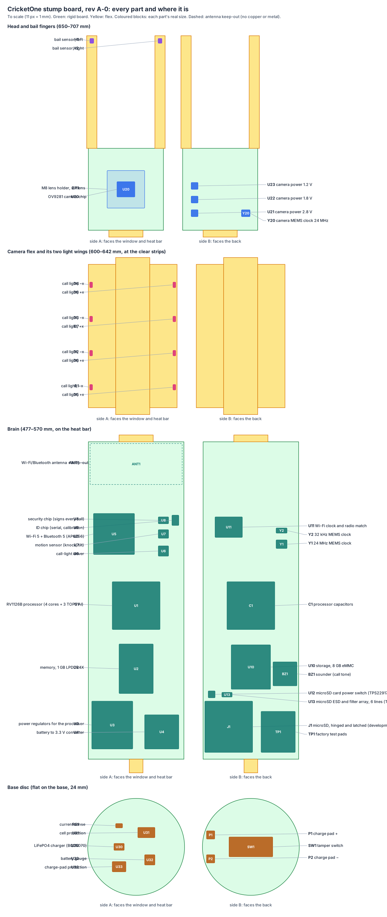
Height is in mm above the grass. Across is mm from the stump’s centre line. Side A faces the window and the heat bar; side B faces the back.
| Ref | Part | Section, side | Height (mm) | Across (mm) | Size (mm) |
|---|---|---|---|---|---|
| H1 | TI DRV5032 Hall switch (X2SON 1.1 × 1.4), left bail, in the head’s Hall pocket | left Hall finger, side A | 705.5 | -10 | 1.1 × 1.4 |
| H2 | TI DRV5032 Hall switch (X2SON 1.1 × 1.4), right bail, in the head’s Hall pocket | right Hall finger, side A | 705.5 | +10 | 1.1 × 1.4 |
| U23 | Camera LDO 1.2 V (core) | head, side B | 663 | -7.5 | 2 × 2 |
| LH1 | M8 lens holder over the camera chip (2 screws), Ø7 lens through the head’s Ø9 window bore | head, side A | 662 | 0 | 11 × 11 |
| U20 | OmniVision OV9281 global-shutter camera chip | head, side A | 662 | 0 | 5.24 × 4.46 |
| U22 | Camera LDO 1.8 V (I/O) | head, side B | 659 | -7.5 | 2 × 2 |
| U21 | Camera LDO 2.8 V (analog) | head, side B | 655 | -7.5 | 2 × 2 |
| Y20 | Camera 24 MHz MEMS oscillator (shock-rated) | head, side B | 655 | +7.5 | 2.5 × 2 |
| D4 | Call light, side-emitting LED shining −x into the clear strip (z 636) | −x light wing, side A | 636 | -12.2 | 0.8 × 1.6 |
| D3 | Call light, side-emitting LED shining −x into the clear strip (z 626) | −x light wing, side A | 626 | -12.2 | 0.8 × 1.6 |
| D2 | Call light, side-emitting LED shining −x into the clear strip (z 616) | −x light wing, side A | 616 | -12.2 | 0.8 × 1.6 |
| D1 | Call light, side-emitting LED shining −x into the clear strip (z 606) | −x light wing, side A | 606 | -12.2 | 0.8 × 1.6 |
| D8 | Call light, side-emitting LED shining +x into the clear strip (z 636) | +x light wing, side A | 636 | +12.2 | 0.8 × 1.6 |
| D7 | Call light, side-emitting LED shining +x into the clear strip (z 626) | +x light wing, side A | 626 | +12.2 | 0.8 × 1.6 |
| D6 | Call light, side-emitting LED shining +x into the clear strip (z 616) | +x light wing, side A | 616 | +12.2 | 0.8 × 1.6 |
| D5 | Call light, side-emitting LED shining +x into the clear strip (z 606) | +x light wing, side A | 606 | +12.2 | 0.8 × 1.6 |
| ANT1 | Wi-Fi/BT chip antenna in a 28 × 12 keep-out (z 558–570, above the heat bar) | brain, side A | 564 | 0 | 27 × 12 |
| U8 | ATECC608B security chip | brain, side A | 547 | +8 | 3 × 2 |
| U9 | ID EEPROM 2 kbit | brain, side A | 547 | +11.5 | 2 × 3 |
| U11 | Wi-Fi 26 MHz / 32 kHz and RF match | brain, side B | 545 | -6.5 | 8 × 6 |
| Y2 | 32.768 kHz MEMS oscillator for the clock (shock-rated) | brain, side B | 544 | +9 | 3.2 × 1.5 |
| U5 | AMPAK AP6256 Wi-Fi 5 + Bluetooth 5 module (certified) | brain, side A | 543 | -6.5 | 12 × 12 |
| U7 | LSM6DSOX motion sensor | brain, side A | 543 | +8 | 3 × 2.5 |
| Y1 | 24 MHz MEMS oscillator (rated to 50,000 g; a quartz crystal is not rated for ball hits) | brain, side B | 540 | +9 | 3.2 × 2.5 |
| U6 | Call-light driver, 12-channel constant current (I2C) | brain, side A | 538 | +8 | 3 × 3 |
| U1 | Rockchip RV1126B-P, FCCSP-409, 0.65 mm pitch | brain, side A | 522 | 0 | 14 × 14 |
| C1 | RV1126B decoupling field (under the chip) | brain, side B | 522 | 0 | 14 × 14 |
| U10 | eMMC 5.1 8 GB industrial, 153-ball FBGA, shipped empty so the card always starts first | brain, side B | 504 | 0 | 11.5 × 13 |
| U2 | LPDDR4X 8 Gbit ×32 (1 GB), 200-ball FBGA | brain, side A | 504 | 0 | 10 × 14.5 |
| BZ1 | Sounder, 7 × 7 magnetic buzzer (the call tone), out through a port in the top sleeve | brain, side B | 502 | +10 | 7 × 7 |
| U3 | Power: multi-rail regulators for the RV1126B (core, NPU, logic, DDR, 1.8/3.3 V) + inductors | brain, side A | 487 | -7 | 12 × 14 |
| J1 | microSD socket with a hinged, latched lid (a push-push socket can eject on a ball hit); fitted on every board: our software starts from the card | brain, side B | 487 | -6.5 | 14 × 15 |
| U13 | microSD ESD and filter array, 6 lines, 22 Ω series resistors | brain, side B | 496 | -7 | 3 × 1.35 |
| U12 | microSD card power switch (TPS22917-class), 10 kΩ discharge | brain, side B | 496 | -11.5 | 2 × 2 |
| U4 | Buck-boost 2.5–3.6 V cells to 3.3 V system (TPS63020-class, 3 × 4) + inductor | brain, side A | 485 | +7.5 | 10 × 10 |
| TP1 | Factory pads: USB 2.0 (writing software), debug serial, boot, rails, current sense | brain, side B | 485 | +8 | 10 × 12 |
| BT4 | Cell pads: cell 3 + and the cell thermistor, stiffened | tail flex, side A | 234 | 0 | 3.4 × 8 |
| BT3 | Cell pads: cells 2 / 3 join (nickel tabs), stiffened | tail flex, side A | 169 | 0 | 3.4 × 6 |
| BT2 | Cell pads: cells + / − join (nickel tabs), stiffened | tail flex, side A | 101 | 0 | 3.4 × 6 |
| BT1 | Cell pads: cell 1 − (nickel tab), stiffened | tail flex, side A | 32 | 0 | 3.4 × 6 |
| RS1 | Current-sense resistor | base disc, side A | 24 (flat) | -5 | 2 × 1.25 |
| U31 | 1-cell LiFePO4 protector (2.5 V cut-off, over-current, short) + dual FET | base disc, side A | 24 (flat) | +3 | 5 × 3 |
| P1 | Charge landing pad + (the base’s spring pin presses here) | base disc, side B | 24 (flat) | -11.8 | 2.4 × 2.4 |
| U30 | TI BQ25070 LiFePO4 charger, 1 A (2 × 3 WSON) | base disc, side A | 24 (flat) | -5 | 3 × 2 |
| SW1 | Omron D2F-01 tamper switch (in the base pocket) | base disc, side B | 24 (flat) | 0 | 12.8 × 5.8 |
| P2 | Charge landing pad − | base disc, side B | 24 (flat) | -11.8 | 2.4 × 2.4 |
| U32 | Battery gauge, coulomb counting (MAX1726x-class) | base disc, side A | 24 (flat) | +4 | 3 × 3 |
| U33 | Charge-pad input: reverse/surge protection + ideal diode | base disc, side A | 24 (flat) | -5 | 4 × 3 |
1. The shape: one board, folded into the stump
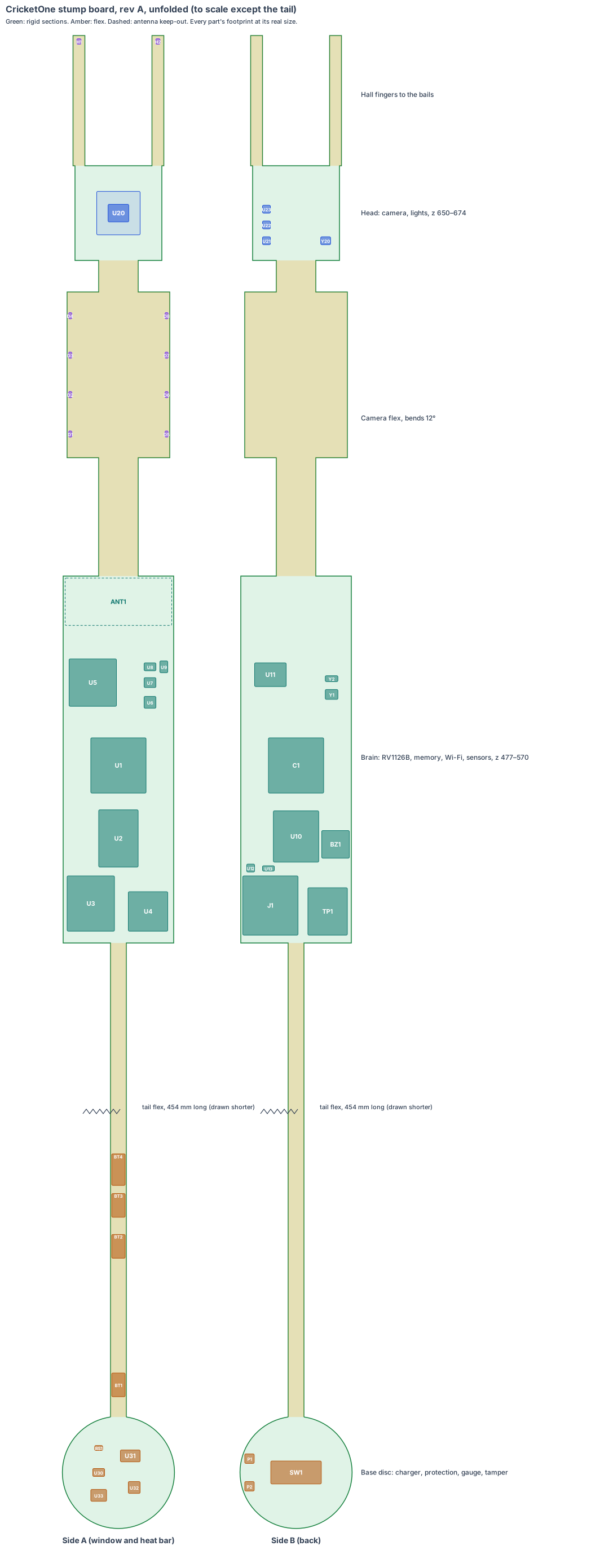
Unfolded, the board is a spine of five rigid and flexible sections:
| Section | Type | Size | Where it sits in the stump | What is on it |
|---|---|---|---|---|
| Head | rigid, 4 layers | 22 × 24 mm | in the head’s camera slot behind the window, z 650–674, tilted 12° | the OV9281 camera chip under an M8 lens holder (Ø7 lens), camera power and clock |
| Hall fingers (2) | flex | 3 × 33 mm | up into the head’s two Hall pockets (x ±10, 705.5 mm); the outer stumps have one finger at the centre | one Hall switch (DRV5032) at each tip, under the bail’s magnet |
| Camera flex | flex, 2 layers | 10 × 80 mm | z 570–650; bends 12° into the head | the camera’s 2-lane signal, power and control; two light wings (8 × 42 mm) carry 8 side-facing LEDs into the clear strips at ±x, 600–642 mm |
| Brain | rigid, 8 layers (HDI) | 28 × 93 mm | on the heat bar, z 477–570 | RV1126B, 1 GB memory, 8 GB storage, power, Wi-Fi/Bluetooth and its antenna, motion sensor, security chip, ID chip, light driver |
| Tail | flex, 2 layers | 4 × 453 mm | in the cell carrier’s 5 mm back wire channel, past the two cells, z 24–477 | battery power and the gauge’s signal; stiffened pads where the cells’ nickel tabs are soldered |
| Base disc | rigid, 4 layers | Ø 28.4 mm | flat on the base, z 24 | charge-pad input, LiFePO4 charger, cell protection, battery gauge, tamper switch, charge landing pads |
Why this shape:
- The bore is 31.75 mm and the carrier’s core is 28.4 mm, so the brain is 28 mm wide on the stump’s centre line, with room for chips on both sides.
- The heat bar runs z 477–557, so the antenna end (z 558–570) sits above it, where the glass-fibre tube passes radio.
- The cells stay low in the stump, and the tail flex reaches them.
- The disc lies on the base, where the charge pads and the tamper pocket are.
2. What is on the brain
| Ref | Part | Size (mm) | Side |
|---|---|---|---|
| U1 | Rockchip RV1126B-P, 0.65 mm-pitch ball package; a thermal pad joins it to the heat bar | 14 × 14 | window |
| U2 | LPDDR4X memory, 1 GB, right next to U1 (short memory lines) | 10 × 14.5 | window |
| U10 | eMMC storage, 8 GB industrial, under U2 | 11.5 × 13 | back |
| U3 | power regulators for the chip’s core, AI engine, logic, memory and I/O, from one 3.3 V input | 12 × 14 zone | window |
| U4 | buck-boost: cells (2.5–3.6 V) to 3.3 V | 10 × 10 zone | window |
| U5 | AMPAK AP6256 Wi-Fi 5 + Bluetooth 5 module (already certified) | 12 × 12 | window |
| ANT1 | chip antenna in a 27 × 12 mm keep-out, above the heat bar | window | |
| U6 | 12-channel light driver for the call lights | 3 × 3 | window |
| U7 | LSM6DSOX motion sensor (knock, tilt, stump hit) | 3 × 2.5 | window |
| U8 | ATECC608B security chip (signs every call) | 3 × 2 | window |
| U9 | ID chip: product, board version, serial, calibration | 2 × 3 | window |
| J1 | microSD slot with a hinged, latched lid, on every board: our software is on the card | 14 × 15 | back |
| U12 | card power switch: the processor can power-cycle a stuck card | 2 × 2 | back |
| U13 | card ESD and filter array, with 22 Ω series resistors on the card lines | 3 × 1.35 | back |
| TP1 | factory pads: USB for writing software, debug serial, boot, power rails | 10 × 12 | back |
Every board starts from the microSD card (owner, 4 Nov 2026): put the card in, switch on, and it starts our program. How the design makes sure of it:
- The RV1126B tries its start devices in a fixed order: SPI flash, then eMMC, then the card, then USB. An image on the eMMC would start before the card, so the eMMC ships empty and the loader on our card is set to read the card first. The eMMC is kept for recordings and logs.
- The card has its own power switch (U12), so the processor can restart a stuck card without restarting the stump. It also has ESD protection (U13) and 22 Ω series resistors, because the slot is the one place a person touches the electronics.
- The lid is hinged and latched, so a ball hit cannot eject the card. The card is an industrial pSLC one (Kingston Industrial or Swissbit), rated −40 to 85 °C.
- The card holds a read-only system with a separate data partition, so a power cut cannot damage the system. Updates over Wi-Fi write the second system copy, and a bad update rolls back by itself.
- On the card: the start loader at sector 64, U-Boot at sector 16384, then the system and data partitions. Writing a card is one step on a PC.
- Signed calls do not depend on the card: the key stays in the security chip (U8), and the card’s system is signed.
3. The camera, built on the board
- The OmniVision OV9281 global-shutter camera chip (5.24 × 4.46 mm, datasheet v1.22) is soldered on the head section, in the same slot the CAD kept for the camera board (24 × 25 mm at 662 mm).
- An M8 lens holder with a Ø7 lens goes over it. An M12 lens would not pass the head’s Ø9 window bore. The lens is chosen by the camera-view simulations for the 12° view from 662 mm.
- The camera’s 2.8, 1.8 and 1.2 V regulators and the 24 MHz clock sit on the back of the head.
- The camera’s signal reaches the RV1126B through the board’s own flex section. There is no camera cable to fit, reverse or shake loose, which removes the failure that overheated our bench board on 3 Nov 2026.
4. The battery system, built on the board
| Ref | Part | What it does |
|---|---|---|
| U33 | pad input protection + ideal diode | the charge pads at the grass line survive being wet, shorted or reversed |
| U30 | TI BQ25070 LiFePO4 charger, 1 A, 2 × 3 mm | the charge voltage is fixed inside the chip, so nothing is set by hand (the bench charger came set to the wrong voltage) |
| U31 | 1-cell LiFePO4 protector + dual switch | cuts off at about 2.5 V, on over-current and on a short (the bench pack had no protection) |
| U32 | battery gauge (coulomb counting) | a LiFePO4 cell’s voltage barely changes until it is nearly flat, so it counts charge in and out |
| BT1–BT3 | stiffened pads on the tail | the cells’ nickel tabs and thermistor are soldered on, with no connector; no charging below 0 °C or above 45 °C |
| SW1 | Omron D2F-01 tamper switch | soldered under the disc, into the base pocket |
| P1, P2 | charge landing pads | the base’s spring pins press on them, so the inside case still slides out on its cord |
Power budget (rev T, board review):
- The cells: three 3.4 Ah LiFePO4 26650 cells (1S3P, the third bay of the cell carrier).
- A 10-hour day: 8 h of play (700 balls) and 2 h of breaks uses about 13 Wh. That is 2.8 W in each delivery, 1.3 W between balls (camera at 60 fps, AI engine asleep) and 0.55 W in breaks.
- Run time, worst case (aged cells at 5 °C): 13.8 h.
- Why three cells: two A123 cells gave only 6.1 h worst case and 9.1 h new.
The dev kit and rev A measurements replace these estimates.
5. Heat
- The RV1126B draws about 1.5–2.5 W at full camera and AI load (est.).
- Its heat path: a 1 mm thermal pad, then the aluminium heat bar (z 477–557), then the tube wall.
- No bought heatsinks: the pad and the bar are in the CAD.
- Rev A logs its temperature from the first power-on.
6. Factory test (every board, every time)
- Current-limited first power-on (100 mA). A short trips in about 1 s, before anything heats.
- Every power rail within ±3 %, and the charger at its set voltage into a test load.
- A factory card goes in and the board starts from it, with the eMMC left empty. The card power switch is tested by cutting and restoring the card supply.
- Camera frame from a test chart (focus, exposure, frame rate). Then Wi-Fi, the motion sensor, the lights read by a light sensor, both bail sensors with a magnet, and the tamper switch.
- Cell protection trips at low voltage and on a short; the gauge and thermistor read correctly.
- The unit’s own key goes into the security chip, the ID chip is written and the label is printed. Every result is stored against the serial number.
7. Who makes what
| Work | Who |
|---|---|
| Board shape, parts, placement, checks, KiCad files, schematics | IEMI Labs |
| The RV1126B memory and power layout (the hardest part) | started from Rockchip’s hardware design guide and reference schematic (through Rockchip’s distributor), then laid out or reviewed by an engineer experienced with Rockchip boards |
| The board (8-layer HDI brain + flex sections, one rigid-flex piece) | a rigid-flex maker (e.g. PCBWay); JLCPCB makes flex but not rigid-flex today |
| Assembly with X-ray of the ball-grid chips | the same maker or a Shenzhen assembly house |
| Software: Linux from Rockchip’s RV1126B SDK, our camera driver and tracking, the product program | IEMI Labs; developed on an RV1126B development kit while the board is made |
8. Cost per stump, electronics (est.)
| qty 10 (rev A) | qty 1,000 | qty 10,000 | |
|---|---|---|---|
| Chips and parts | $125–150 | $55–65 | $45–52 |
| Rigid-flex board | $60–120 | $10–14 | $7–9 |
| Assembly (incl. X-ray) | $30–50 | $4–6 | $3–4 |
| Per stump | $215–320 | $69–85 | $55–65 |
Rev A is dear because a few rigid-flex boards cost a lot to make. From about 1,000 boards the single board is cheaper than any bought-board build, and it needs no hand assembly.
9. Timeline
| When | Step |
|---|---|
| Nov 2026 | RV1126B development kit; Rockchip hardware design guide; our camera and tracking code running on the kit |
| Nov–Dec 2026 | schematics from the reference design; placement (this drawing) into KiCad; engineer review of the memory and power layout |
| Jan 2027 | rev A layout done and checked; boards ordered (rigid-flex about 2–3 weeks) |
| Feb 2027 | rev A bring-up on our fixture; drop and ball-hit tests |
| Mar–Apr 2027 | rev B (fixes) and factory test software; pilot wickets |
| from May 2027 | certification, then first sales |
10. CAD check (rev T, 3 Nov 2026)
The board is placed in the stump CAD (products/cricketone/cad/cricketone-t-cad.mjs). That script loads every rev S printed part and every bought part that stays, puts the folded board in all three stump types (middle, leg, off), and checks every board part against all of them:
- No board part touches a bought part: cells, heat bar, window, light strips, button, pads, vent.
- Where the board needs room in a printed part, a 0.3 mm clearance pocket is cut:
| Part | Material removed |
|---|---|
| Camera bracket | 4–5 % |
| Top carrier | 2.5 % |
| Cell carrier | 1.3 % |
| Head top | 0.3–0.5 % |
| Top sleeve | 0.2 % |
- Rev T changes found by the check:
- The base’s spring pins move from x −14.2 to x −11.8, onto the disc’s charge pads.
- The Hall-tamper post goes; the board’s tamper switch does that job.
- The heat bar shortens to 75 mm (477–552 mm), so no metal is within 5 mm of the antenna. It is bonded to the processor with a thermal adhesive pad.
- The bar’s old screw holders, which the brain cut loose, are gone. The brain is held in card guides.
- A sounder port goes through the top carrier and sleeve.
11. Still to check
- The RV1126B-P’s power rails, from Rockchip’s hardware design guide (the Boardcon module runs it from a single 3.3 V input, which this design follows).
- The camera driver for the OV9281 in Rockchip’s SDK, on the development kit.
- The LiFePO4 protector chip and its exact cut-off voltages.
- The rigid-flex maker’s limits for the 453 mm tail.
- The card-guide hold of the brain under the drop and ball-hit tests (rev T).
- The antenna’s range with the aluminium collar 2.6 mm above it (RF test).