CricketOne test board: the circuit
4 November 2026, rev A-1. This is the first real circuit of our board: every part, every pin, and what each pin connects to. KiCad’s electrical rule check (ERC) passes it with 0 errors. Until today our board was only a plan of where parts sit (see where the board stands).
Schematic (PDF) · KiCad files, parts list and netlist (zip)
1. Three boards, soldered together
The test board takes route 1 of the board plan: the processor comes on a module, soldered flat onto our own plain 4-layer boards that any local shop can make.
| Board | Where in the stump | What is on it |
|---|---|---|
| Main board | the middle, on the heat bar | the Boardcon LGA1126B module (RV1126B, 2 GB memory, 8 GB eMMC), power, the microSD card, Wi-Fi and Bluetooth, motion sensor, security chip, ID chip, the call-light driver, the tone, factory pads |
| Camera head | at the window | the OV9281 camera chip and its three supplies, the M8 lens holder, the 8 call lights, the two bail sensors |
| Base board | on the cells | the LiFePO4 charger, cell protection, fuel gauge, cell thermistor, tamper switch, charge pads |
They are joined by soldered leads, not plugs: a 30-way 0.5 mm flex between the main board and the camera head, soldered at both ends, and an 8-wire lead down to the base board. A ball hit cannot unplug them.
2. Put the card in, switch on, it starts
- The module’s eMMC ships empty. The RV1126B tries the eMMC before the card, so an empty eMMC means the card always wins.
- The card sits in a hinged, latched socket (J1).
- Its supply has its own power switch (U4): the processor can restart a stuck card, and the card supply drops to 0 V when off.
- An ESD and filter array (U5) protects all six card lines. The pull-ups go to the card supply, so a switched-off card is never fed through them.
- There is no other setup. USB, the debug console and the Maskrom pad are factory pads only, for a spring-pin fixture.
3. What each block does
- Power. Three 3.4 Ah LiFePO4 cells in parallel (2.5–3.6 V):
- a TPS61022 boost makes 5.0 V for the module (it needs 3.1–5.5 V);
- a TLV62568 buck makes 3.3 V for everything else;
- the module’s own 1.8 V output runs the camera signals.
- Wi-Fi and Bluetooth: AMPAK AP6256, a certified module.
- SDIO at 3.3 V, Bluetooth on UART1, 32.768 kHz from the module. The module’s pins are already named for it.
- Its 37.4 MHz clock is a MEMS oscillator instead of the usual quartz crystal, which is not rated for ball hits.
- Chip antenna in its keep-out, with a π match tuned on the first boards.
- Camera: OV9281, 2-lane MIPI to the module’s RX0 port.
- The clock (MCLK), camera I2C, frame-sync (FSIN), reset and power-down, all at 1.8 V.
- Its own LDOs: 2.8 V (AVDD), 1.8 V (DOVDD) and 1.2 V (DVDD).
- Sensors and chips on one I2C bus:
- LSM6DSOX motion sensor, for ball hits and the stump being knocked;
- ATECC608B security chip, which signs every call;
- 24AA02 ID chip;
- IS31FL3216 call-light driver;
- MAX17260 gauge, on the base board, up the lead.
- Bails: two DRV5032FA Hall switches (20 Hz, 1.3 µA). They say a bail is off; the camera gives the exact time.
- Charging: BQ25070, the LiFePO4 charger, from the 5 V charge pads.
- Its current is set by pulses on a control pin, so it is wired up the lead.
- The processor sets 935 mA. With the processor off it charges at 285 mA.
- Protection: a DW01A with a dual FET cuts off on a short, on over-current, and on over-discharge at 2.4 V. The charger’s own fixed 3.6 V limit stops over-charge.
4. Still to confirm before layout
The circuit is drawn and checked by ERC. These items are checked against the full datasheets or reference designs before any copper is drawn:
- OV9281 ball map and pitch. The balls come from Antmicro’s open-source OV9281 board. OmniVision’s datasheet (through a distributor) confirms every ball, the package size, the power-up order and the internal supply pins (PVDD, VH, VN1–VN3, each with 1 µF for now).
- The module’s pads. Our reading of Boardcon’s pin table lists 240 pads; Boardcon calls the module LGA238. The footprint is drawn from Boardcon’s drawing and checked pad by pad.
- AP6256 buck inductor. Which end of L4 goes to pin 21 and which to pin 23, from AMPAK’s reference design.
- 37.4 MHz oscillator. Its accuracy (±10 ppm) and output level into the AP6256 XTAL_IN pin.
- Fuel gauge. The MAX17260 pins (drawn with the MAX17261 symbol), the sense-resistor side and the LiFePO4 model.
- Cell protection. The FS8205A pins, and whether a protector with LiFePO4 thresholds replaces the DW01A.
- LED current (R21) and the buzzer at 5 V with PWM.
- The power budget at the module’s peak, on the dev kit.
5. The layout (started 4 Nov 2026)
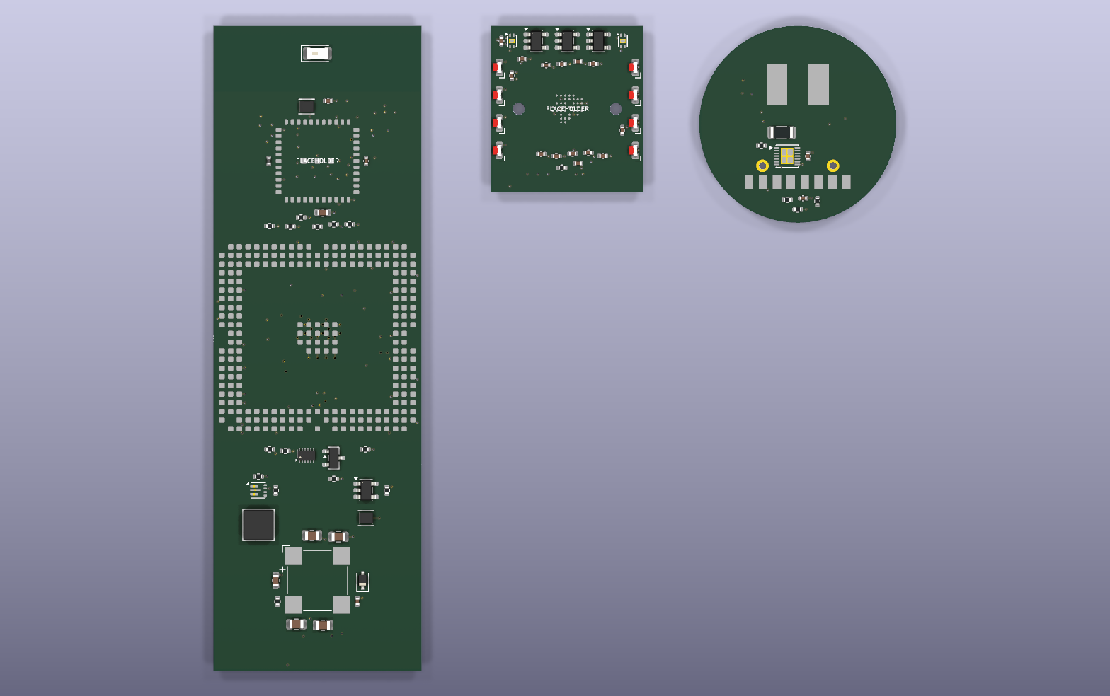
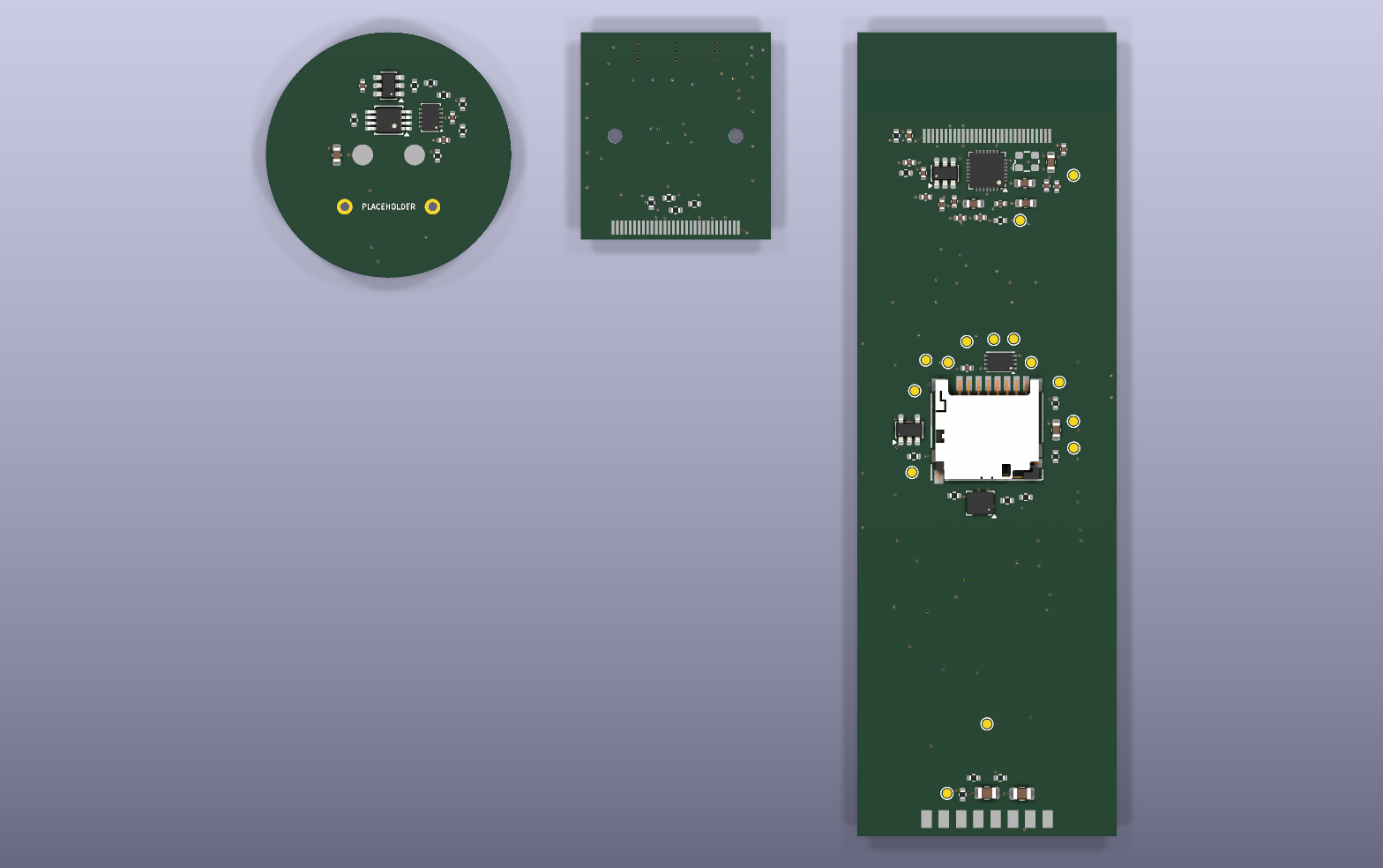
The three boards are now real KiCad board files (board file and renders in the zip):
- 153 footprints with 835 pads, each pad on its net from the schematic, on a 4-layer stack-up;
- the module under the heat bar, the Wi-Fi module and antenna at the top end with a 9.5 mm keep-out, the microSD socket on the back;
- the camera chip at the window with the lens holder over it, the call lights at the strips;
- the cell pads, charger and gauge on the base disc;
- every small part placed next to the chip it serves.
KiCad’s design rule check: 0 errors in spacing, courtyards or holes. Still open:
- the connections to route (section 6);
- 27 silkscreen notes, which are cosmetic: library outlines over pads, trimmed by the maker.
The main board is 30 mm wide (it was 28 mm) so that the 28.75 mm module fits. On paper that leaves 5.2 mm each side of the centre plane at the board’s edges in the 31.75 mm bore. It is checked in the stump CAD (rev U) before routing.
4 of our 9 footprints are placeholders, marked PLACEHOLDER on the board. Each is redrawn from the maker’s drawing before routing:
- the AP6256 pads;
- the OV9281 ball pitch;
- the lens holder screw spacing;
- the D2F tamper switch pins.
Footprints from KiCad’s own library: the hinged microSD socket (Hirose DM3D-SF), the TI packages, the buzzer and every small part.
6. Routing (started 4 Nov 2026)
Step 1, the planes, done:
- a solid ground plane on inner layer 1 under all three boards;
- the 3.3 V plane on inner layer 2 (main board and camera head; ground again on the base disc);
- 192 vias, one beside each ground and 3.3 V pad, with a short track to the pad. There are no vias in pads, since those would need filled vias, and none in the antenna’s copper-free zone or under the card socket.
KiCad’s design rule check now finds 0 copper errors: no clearance, short, hole or keep-out violations. The 27 cosmetic silkscreen notes remain.
Connections: 183 of 499 made, 316 to route:
| Kind | Left | How |
|---|---|---|
| Ground and 3.3 V pads with no room for a via yet (mostly between the module’s pads) | 48 | short tracks to a neighbouring via |
| Fast signals: camera lanes, USB, microSD card, Wi-Fi SDIO, antenna | 71 | impedance-matched: camera 100 Ω pairs, USB 90 Ω, antenna 50 Ω, length-matched card and SDIO lines |
| Other power: 5 V, battery, card supply, camera supplies | 72 | wide tracks |
| Slower signals: I2C, lights, control, lead and flex | 125 | auto-router |
The auto-router. The open-source router Freerouting 2.5.0 was tried on the board and reached its first pass with 0 violations. Its Windows build has a bug that crashes it before it can save. The standard version needs a Java 25 runtime, a separate download, so it was not run here. The board is also exported in the router’s format (test-board.dsn in the zip), so a layout engineer or a later run can pick it up.
Next:
- Route the 71 fast signals by hand, or with a layout engineer: they decide the camera’s image quality and the card’s speed.
- Auto-route the rest, then KiCad’s design rule check with 0 unconnected.
- Gerbers, drill files, placement file, assembly drawings and the IPC-356 netlist. Then the quote requests go out with real files.
7. The parts
Every part on the three boards, grouped by part. Test pads are not listed.
| Refs | Qty | Part | Maker part | Note |
|---|---|---|---|---|
| U1 | 1 | Boardcon LGA1126B (2 GB / 8 GB) | Boardcon LGA1126B-2G8G | module: RV1126B, LPDDR4X, eMMC, power; 3.1–5.5 V in |
| C1 C2 C6 C7 C8 C9 | 6 | 22u | 22u X7R/X5R 0805 | module input bulk, next to A2/A3/B1/B3 |
| C3 C5 C16 C29 C18 C22 C23 C24 C25 C32 C34 C36 C37 C38 C40 C42 | 16 | 100n | 100n X7R/X5R 0402 | |
| C4 C14 C26 C39 C46 C47 C48 C49 C30 C31 C33 C35 C41 | 13 | 1u | 1u X7R/X5R 0402 | module 1.8 V out, 400 mA max |
| R1 R14 R15 R16 R17 R18 R23 R24 R33 R34 | 10 | 10k | 0402 10k 1 % | PWR_EN has 10k inside; this keeps it on at power-up |
| U2 | 1 | TPS61022 | TPS61022RWUR | boost 1.8–5.5 V in to 5.0 V, 8 A switch; TI SLVSF60 typical application |
| L1 | 1 | 1u | Coilcraft XAL4020-102MEB (1 µH, 9.6 A sat) | |
| R2 | 1 | 732k | 0402 732k 1 % | 5.0 V = 0.6 V × (1 + 732k/100k) |
| R3 R4 R6 R7 R13 R22 R47 R49 R50 R43 | 10 | 100k | 0402 100k 1 % | |
| U3 | 1 | TLV62568 | TLV62568DBVR | buck 5 V to 3.3 V, 1 A; TI SLVSDE6 typical application |
| L2 | 1 | 2.2u | Murata DFE201610E-2R2M (2.2 µH) | |
| R5 | 1 | 453k | 0402 453k 1 % | 3.32 V = 0.6 V × (1 + 453k/100k) |
| C10 C27 C19 | 3 | 4u7 | 4u7 X7R/X5R 0603 | |
| C11 C12 C15 C17 | 4 | 10u | 10u X7R/X5R 0603 | |
| J1 | 1 | microSD, hinged | Hirose DM3D-SF (hinged lid that latches shut) | a push-push socket ejects on a ball hit; card detect switch to GND |
| U4 | 1 | TPS22917 | TPS22917DBVR | card power switch: the processor can restart a stuck card; quick output discharge |
| R25 | 1 | 100R | 0402 100R 1 % | quick output discharge: the card supply falls to 0 V when switched off (TI: QOD to VOUT, a resistor sets the rate) |
| C13 | 1 | 1n | 1n X7R/X5R 0402 | slow turn-on (about 0.4 ms), no dip on 3.3 V |
| U5 | 1 | TPD6F003 | TPD6F003DQDR | ESD + EMI filter, 6 lines: TI recommends it for SD/SDIO |
| R8 R9 R10 R11 R12 | 5 | 47k | 0402 47k 1 % | SD pull-ups to the card supply, so a switched-off card is not fed through them |
| U6 | 1 | AP6256 | AMPAK AP6256 | AMPAK AP6256 datasheet rev 1.0 §7.2 (47 pins); cross-checked with the Pinebook Pro v2.1 mainboard schematic sheet 17 |
| L4 | 1 | 3.3u | 3.3 µH 0806 (as the Pinebook Pro AP6256 circuit) | AP6256 internal buck: which end goes to pin 21 or 23 to confirm with the AMPAK reference |
| Y1 | 1 | 37.4 MHz MEMS | SiTime SiT8008BI-12-33E-37.400000 (±10 ppm needs the SiT8208/SiT8209 class: to confirm) | replaces the AP6256 37.4 MHz quartz crystal: rated for ball hits |
| C28 | 1 | 10p | 10p X7R/X5R 0402 | couples the oscillator into XTAL_IN (clipped-sine input level to confirm) |
| C20 C21 | 2 | DNP (not fitted) | π match, fitted after tuning | |
| L3 | 1 | 0R | 0402 0 Ω (π match series, tuned on rev A) | |
| AE1 | 1 | 2.4 GHz chip antenna | Johanson 2450AT18A100E | keep-out: no copper, no metal, 27 × 12 mm |
| U7 | 1 | LSM6DSOX | ST LSM6DSOXTR (same LGA-14 pins as LSM6DSL) | ball hits, the stump knocked; I2C address 0x6A (SA0 low) |
| U8 | 1 | ATECC608B | Microchip ATECC608B-MAHDA-T (UDFN-8) | signs every call |
| U9 | 1 | 24AA02 | Microchip 24AA02T-I/OT | ID chip: product, board version, serial, calibration |
| R19 R20 | 2 | 2k2 | 0402 2k2 1 % | I2C pull-ups, 400 kHz |
| U10 | 1 | IS31FL3216 | Lumissil IS31FL3216-QFLS2-TR | 16-channel constant-current LED driver, I2C 0x74 |
| R21 | 1 | 3k3 | 0402 3k3 1 % | sets the full-scale LED current (about 20 mA; Lumissil datasheet table) |
| BZ1 | 1 | magnetic buzzer | CUI CMT-8504-100-SMT (8.5 × 8.5 mm, 5 V, 100 dB at 10 cm) | the call tone, out through a port in the top sleeve |
| Q1 | 1 | BSS138 | onsemi BSS138 | |
| D1 | 1 | BAT54 | Nexperia BAT54HT1 (SOD-323) | catches the buzzer coil kick |
| J2 | 1 | flex pads, 30 × 0.5 mm | pads for a 30-way 0.5 mm FFC, hot-bar soldered (Molex 15020-0306 class) | |
| J20 | 1 | flex pads, 30 × 0.5 mm | pads for the same flex at the head end | |
| U20 | 1 | OV9281 | OmniVision OV09281 (CSP) | ball map from Antmicro’s open-source OV9281 dual camera board (openhardware.antmicro.com); supplies from the Leopard LI-OV9281-MIPI spec. To confirm every ball and the pitch against the OmniVision OV9281 datasheet before layout |
| U21 | 1 | TLV75528 | TLV75528PDBVR | camera analog 2.8 V |
| U22 | 1 | TLV75518 | TLV75518PDBVR | camera I/O 1.8 V (the same level as the module camera pins) |
| U23 | 1 | TLV75512 | TLV75512PDBVR | camera core 1.2 V |
| R30 R31 | 2 | 4k7 | 0402 4k7 1 % | camera I2C pull-ups to the module 1.8 V |
| R32 R42 R44 R45 | 4 | 0R | 0402 0R 1 % | reset and shutdown share one pin; PWDN is the spare |
| LH1 | 1 | M8 lens holder | M8 lens holder, 2 × M1.6 screws (lens to agree) | |
| H1 H2 | 2 | DRV5032FA | TI DRV5032FADMRR (20 Hz, push-pull, omnipolar) | left bail; TI DRV5032 datasheet SLVSDC7H, X2SON (DMR) pinout for FA/FB/AJ |
| D11 D12 D13 D14 D15 D16 D17 D18 | 8 | side LED | Kingbright APA1606 side-emitting (to pick colour) | call light 1, left strip |
| U30 | 1 | BQ25070 | TI BQ25070DQCR | TI BQ25070 datasheet SLUSA66, DQC 10-pin SON |
| C43 | 1 | 1u | 1 µF 25 V X7R 0603 | IN: datasheet 0.1 µF minimum, larger against hot-plug ringing |
| C44 | 1 | 1u | 1 µF X5R 0402 | OUT/BAT 1 µF |
| C45 | 1 | 100n | 100 nF X7R 0402 | LDO 0.1 µF |
| R46 R41 | 2 | 1k | 0402 1k 1 % | IMON: 0–1 V for 0–1 A |
| R48 | 1 | 490k | 0402 487k 1 % | TS divider top (datasheet: 490k/100k with no NTC; the cell NTC is read by the gauge) |
| U31 | 1 | DW01A | Fortune DW01A (or a LiFePO4-threshold protector, to confirm) | short and over-current cut-off; over-discharge at 2.4 V suits LiFePO4; over-charge is the charger’s fixed 3.6 V |
| Q30 | 1 | FS8205A | Fortune FS8205A (dual N-FET, common drain) | Fortune FS8205A datasheet, TSSOP-8: pins 1 and 8 common drain, 2-3 source 1, 4 gate 1, 5 gate 2, 6-7 source 2 (to confirm) |
| R40 | 1 | 330R | 0402 330R 1 % | DW01A supply filter |
| U32 | 1 | MAX17260 | Analog Devices MAX17260SETD+T (1-cell; pins drawn with the MAX17261 symbol: to confirm) | charge left in the cells; LiFePO4 model; I2C 0x36; sense resistor side to confirm with the typical application |
| RS1 | 1 | 10m | 10 mΩ 1 % 1206 current sense (Susumu KRL1632) | gauge current sense |
| TH1 | 1 | 10k NTC | Murata NCP15XH103F03RC (10 kΩ, B 3380) | on the cells: charge stops below 0 °C and above 45 °C |
| SW1 | 1 | tamper | Omron D2F-01 (tamper) | opens when the base is taken off |
| BT1 | 1 | 3 × LiFePO4 26650, 1S3P | Power Sonic PSL-FP-IFR26650EC or PLB IFR26650-34D (3.4 Ah) ×3 | soldered nickel tabs |
| J30 | 1 | charge pads | gold pads for the charger pins (no part) | |
| J31 | 1 | lead to the main board | 8-wire lead, soldered both ends (J3 on the main board) | |
| J3 | 1 | lead from the base board | the same lead, main board end |
Made with our circuit code: products/cricketone/hardware/pcb/rev-a1/circuit.mjs writes the KiCad schematic, runs ERC and exports the PDF, the netlist and this list.