AthleticsOne: one circuit board of our own in each finish post
What changed (3 Nov 2026). The rev O finish posts are built from bought boards: a DPTechnics Walter, a Raspberry Pi Zero 2 W and Camera Module 3 on a ribbon, a PowerBoost charger and breakout boards for the lightning, NFC, air, temperature and mic parts, joined by wires. AthleticsOne now gets one circuit board of our own in each post, like CricketOne, with every chip placed straight onto it. An assembly house makes and tests it.
- The chips: Rockchip’s RV1126B processor with its memory and storage, Wi-Fi and Bluetooth, the OV9281 global-shutter camera chip, an ESP32-S3 module that stays awake when the processor sleeps, the call-lamp LEDs and sounder, the security chip, and the battery charger, protection and gauge. The home post adds the LTE-M modem with a soldered eSIM, the AS3935 lightning chip, the PN532 NFC reader with its loop drawn in the board copper, the gun mic, the SHT45 air chip and the PT1000 reader for the black top.
- The shape: a flat base section in the steel base box, then one spine up the post: brain, radio section, camera head and top section, joined by the board’s own flex. A short flex runs under the post to the cells, and a small tab folds onto the start-side wall for the gun mic.
- Both posts carry the same board. The away post leaves the 14 home-only parts unfitted, so there is one design, one test and one software image.
- The starter unit is a separate object you carry to the start, so it has its own small S1 board (ESP32-S3-MINI-1, mic, flash diode, charger).
- The rev O bench posts stay as they are. They prove the calls and the software, which move to this board.
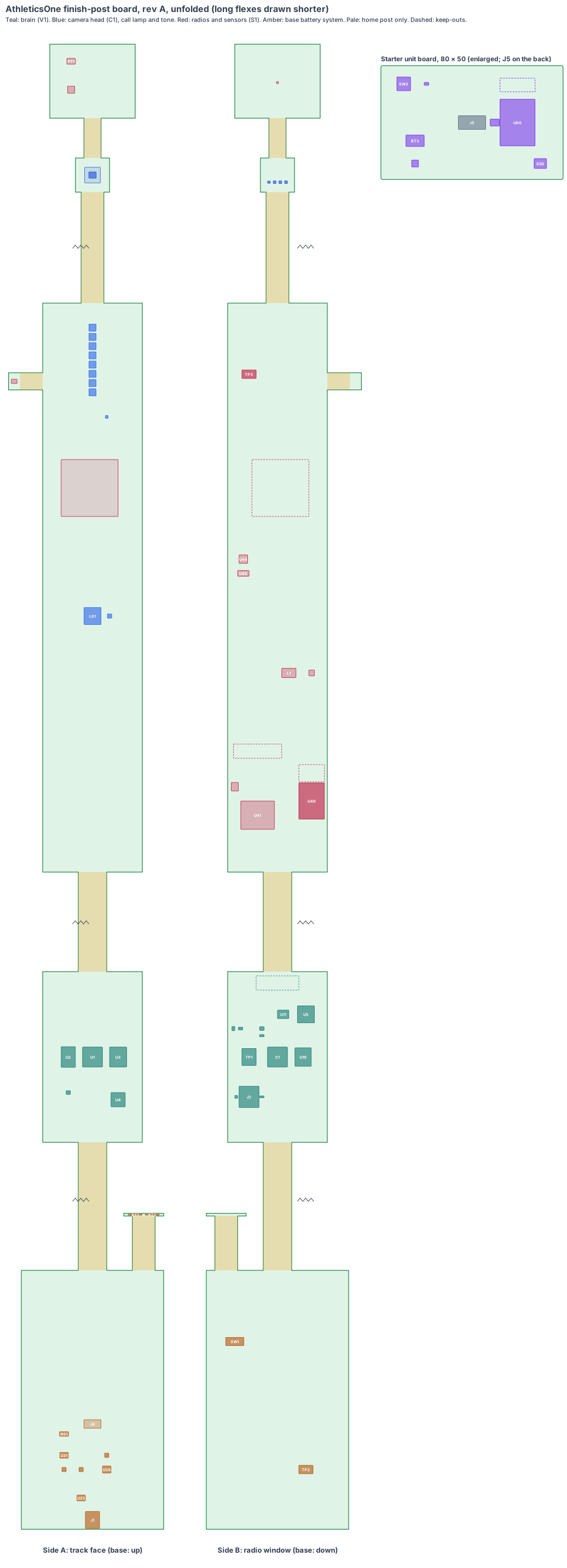
The board is code (hardware/pcb/athleticsone-board.mjs). It writes the KiCad board file (athleticsone-board.kicad_pcb), the parts list (athleticsone-board-parts.csv) and this drawing, and checks every part:
- every part sits inside its section with a 0.3 mm edge margin, no two parts overlap on the same side, and every part’s height fits the space between its side of the board and the post wall;
- the camera chip is on the camera window (z 1,300), the sounder under the tone holes (z 820), the eight lamp LEDs inside the 14 × 54 lamp slot (z 1,000), the air chip behind the vent (z 1,365), the gun mic at its port (z 985) and the dock pins under the starter-unit dock (CAD x −120);
- every antenna (Wi-Fi, ESP32-S3, LTE-M, lightning coil, NFC loop) sits behind the 60 × 600 radio window, z 400–1,000;
- the RV1126B sits on solid track-face wall, away from the windows, for its heat path; the air chip is over 300 mm from every warm part;
- every flex is long enough for its path, and the starter board fits inside its 84 × 54 shell.
KiCad design rule check: 0 violations, 0 unconnected items (KiCad 10, 3 Nov 2026). Each part is drawn at its real size, as a placeholder outline until its full footprint is added.
Sizes come from the post CAD (cad/athleticsone-cad.mjs, rev O: 80 × 20 × 1,400 aluminium post with 2 mm walls, inside 76 × 16; 400 × 250 × 40 steel base box) and the chip datasheets. Numbers marked est. are estimates.
1. The shape: one board, up the whole post
The inside of the post is only 16 mm deep, so every vertical section stands on edge across the post’s 76 mm width, side A to the track face and side B to the back face with its radio window.
| Section | Type | Size (mm) | Where it sits | What is on it |
|---|---|---|---|---|
| Base section | rigid, 4 layers | 100 × 182 | flat in the base box on 10 mm standoffs, z 13 | charger, cell protection, gauge, 5 V boost, the processor’s power switch, M8 charge socket, dock pins (home), tamper switch |
| Cell flex + tab | flex, then rigid 2 layers | 16 × 100, tab 28 × 16 | under the post along the base floor to the four cells | nickel-strip pads for the cell pack and its thermistor |
| Riser | flex, 2 layers | 20 × 390 | bends up out of the base into the post, z 14–380 | power and the brain’s links to the base |
| Brain | rigid, 8 layers (HDI) | 70 × 120 | z 380–500, RV1126B pressed on the track-face wall | RV1126B, 1 GB memory, 8 GB storage, power, Wi-Fi/Bluetooth and antenna, motion sensor, security chip, ID chip |
| Link | flex, 2 layers | 20 × 140 | z 500–640 | brain to the radio section |
| Radio section | rigid, 4 layers | 70 × 400 | z 640–1,040, behind the radio window | ESP32-S3 module, LTE-M modem and eSIM, lightning chip and coil, NFC chip and copper loop (side B); sounder and call lamp (side A) |
| Mic tab | flex then rigid, 2 layers | 16 × 12, tab 8 × 12 | folds onto the start-side wall, z 985 | the gun mic (home) |
| Upper flex | flex, 2 layers | 16 × 248 | z 1,040–1,288 | the camera’s 2-lane signal, power and control |
| Camera head | rigid, 4 layers | 24 × 24 | behind the camera window, z 1,300, tilted 10° down | OV9281 camera chip, M8 lens holder, its regulators and clock |
| Top section | rigid, 4 layers | 60 × 52 | under the cap, z 1,340–1,392 | SHT45 behind the vent, MAX31865 and PT1000 pads (home) |
Why this shape:
- The windows are fixed by the rev O post: camera, lamp and tone on the track face; radio window and vent on the back. Each chip that works through a window sits on the section behind it.
- The processor’s heat goes into the aluminium track face, the post’s largest metal surface, so it sits on side A where that wall is solid (z 380–500).
- Every radio, including the NFC loop drawn in the board’s own copper, faces the 60 × 600 polycarbonate radio window. A thin ferrite sheet behind the loop stops the aluminium track face detuning it (est.).
- The base section is the only part in the steel box, which holds the cells and the battery chips.
Three changes to the post CAD (next CAD revision; nothing is bought for them):
- The PowerBoost board is removed from the base; the base section takes its place on four 10 mm standoffs.
- The tamper switch moves onto the base section’s underside, pressed by a boss on the bolted floor plate (was a separate switch on the floor plate).
- The charge input becomes an M8 3-pin screw-locked socket through the base end wall (was the PowerBoost’s USB socket inside the base), and the home base’s dock gets two sealed brass feedthrough pins for the starter unit.
2. What is on each section
The brain uses the same V1 core as CricketOne (chip, memory, storage, power layout and software image). The camera head uses the same C1 camera chip. The radio section uses the S1 core’s ESP32-S3 module, as on RoomOne. Only what is different for a finish post is described here.
| Ref | Part | Size (mm) | Section, side | Post |
|---|---|---|---|---|
| U1 | Rockchip RV1126B-P, thermal pad to the track-face wall | 14 × 14 | brain, A | both |
| U2, U10 | LPDDR4X 1 GB; eMMC 8 GB industrial | 10 × 14.5; 11.5 × 13 | brain, A; B | both |
| U5, ANT1 | AMPAK AP6256 Wi-Fi 5 + Bluetooth 5 (certified); chip antenna in a 30 × 10 keep-out facing the radio window | 12 × 12 | brain, B | both |
| U8 | ATECC608B security chip (signs every result) | 3 × 2 | brain, B | both |
| U7 | LSM6DSOX motion sensor (knocks, tilt, theft) | 3 × 2.5 | brain, A | both |
| U40, ANT2 | Espressif ESP32-S3-WROOM-1-N8R8 (certified), the always-on brain | 18 × 25.5 × 3.1 | radio, B | both |
| U41, U42, ANT3 | Quectel BG95-M3 LTE-M modem, MFF2 eSIM, 30 × 3 chip antenna | 23.6 × 19.9 × 2.2 | radio, B | home |
| U43, L1 | ScioSense AS3935 lightning chip with its Coilcraft MA5532-AE coil | 4 × 4; 10 × 6.5 (est.) | radio, B | home |
| U44, ANT4, FER1 | NXP PN5321A3HN NFC reader, 40 × 40 copper loop, ferrite sheet behind it | 6 × 6 | radio, B (sheet A) | home |
| LS1, D1–D8 | 12 × 12 magnetic sounder under the tone holes; 8 WS2812B-class LEDs behind the lamp slot | 12 × 12 × 3; 5 × 5 | radio, A | both |
| MK1 | Infineon IM69D130 digital mic over the gun-mic port | 4 × 3 × 1.2 | mic tab | home |
| U20, LH1 | OmniVision OV9281 global-shutter chip, M8 lens holder with a 2.8 mm lens | 5.24 × 4.46; 11 × 11 | head, A | both |
| U52 | Sensirion SHT45 behind the vent | 1.5 × 1.5 | top, B | home |
| U50, PT1 | Analog Devices MAX31865 and the PT1000 lead pads | 5 × 5 | top, A | home |
| U30–U33 | TI BQ24074 charger with power path, cell protection, gauge, input protection | 3 × 3 and zones | base, A | both |
| U34, U35 | TI TPS61023 5 V boost for the lamp and tone; the processor’s load switch | zones | base, A | both |
| J1 | M8 3-pin A-coded PCB socket through the base end wall | 10 × 12 (est.) | base, A | both |
| J4 | two sealed feedthrough pins to the starter-unit dock | 12 × 6 zone | base, A | home |
| SW1 | Omron D2F-01 tamper switch | 12.8 × 5.8 × 6.5 | base, B | both |
All 62 parts, with sizes, heights and sources, are in the parts list.
What the AthleticsOne-only blocks do:
- Two brains, one board. The ESP32-S3 is always on. It works out the heat band every minute, runs the 30-minute lightning clock, reads taps and listens for the gun. It switches the RV1126B on only while a race is armed, as the rev O Walter and Pi did. Then the RV1126B reads the camera at 120 frames a second and makes the finish calls.
- The camera. The OV9281 reads 1,280 × 800 at up to 120 frames a second with a global shutter, so a runner’s torso is not bent by the shutter at the line. A 2.8 mm lens gives about 66° × 44° (est.), which covers the 66° × 41° that the CAD’s 26 view checks need.
- No camera cable, harness or breakout. The board’s own flex carries every signal from the camera, radios, mic and sensors.
3. The starter unit’s board
| Ref | Part | Size (mm) |
|---|---|---|
| U60 | Espressif ESP32-S3-MINI-1-N8 (certified), antenna keep-out at the edge | 15.4 × 20.5 × 2.4 |
| MK2 | Infineon IM69D130 mic, under a printed sound tube to the top port | 4 × 3 |
| D20 | Vishay BPW34 photodiode, under a printed light pipe to the flash window | 5.4 × 4.3 × 3.2 |
| U61, BT3 | Microchip MCP73831 charger; pads for the 500 mAh cell | 3 × 3 |
| SW3, D21 | button and status light | 6 × 6 |
| J5 | two spring pins through the shell floor, landing on the post’s dock pins | 12 × 6 zone |
The board is 80 × 50 × 0.8, 2 layers, on the floor of the 88 × 58 × 20 shell.
4. Every connection, checked
Our rule: every pair of parts that join is checked against both makers’ drawings and a search for known problems. No “same as CricketOne” claims.
| Joint | Type | Keyed | Locked | Check |
|---|---|---|---|---|
| Charge lead ↔ post | M8 3-pin A-coded female PCB socket in the base end wall | yes (A-coding) | the lead’s screw nut | the only connector on the post. The socket’s footprint, panel seal and the lead’s pinout come from one maker’s drawing for both halves (still to check 1). |
| Starter unit ↔ home post | two spring pins on two sealed feedthrough pins, when docked | the dock lip only fits one way round | the unit sits in the 8 mm lip | charging only: no call depends on it. Spring-pin travel and pad size from the chosen maker’s drawing (still to check 2). |
| Camera, radios, mic, lamp, sensors ↔ brain | the board’s own flex | n/a | one piece | none to fit or reverse: this removes the camera ribbon and every breakout wire |
| Cells ↔ base section | nickel strips spot-welded to the cells, soldered to the cell tab | the + and − pads are 12 mm apart and marked | soldered | Samsung 35E drawing; the pack is welded and tested before it is soldered |
| PT1000 ↔ top section | two leads soldered to pads | n/a | soldered | the element’s lead drawing |
| Tamper switch | soldered on the base section | n/a | soldered | the Omron D2F drawing |
No adapters anywhere.
5. Heat
- The RV1126B draws about 1.5–2.5 W at camera and AI load (est.), but only while a race is armed. The ESP32-S3 draws well under 0.5 W most of the time (est.).
- The problem: the post stands in full sun; the aluminium can reach about 60 °C (est.), and the inside is only 16 mm deep.
- The heat path: the chip faces the track face; a 1 mm thermal pad joins it to the 2 mm aluminium wall, and the 80 × 1,360 mm post spreads it. The post is the heat sink.
- The air chip and the PT1000 sit at the top, more than 800 mm above the processor, so its heat does not reach the heat-band readings.
- Rev A logs its temperature from the first power-on. The soak test runs the post at 50 °C ambient under a sun lamp.
6. Power budget (est.)
| Home post | Away post | |
|---|---|---|
| Pack | 4 × Samsung INR18650-35E, 1S4P, 14 Ah, about 50 Wh | the same |
| Idle (ESP32-S3 awake, heat band, lightning clock) | 0.25 W | 0.15 W |
| Race armed (RV1126B, camera 120 fps, Wi-Fi link) | 2.6 W | 2.3 W |
| Call (lamp flash and tone, 2 s) | +1.0 W | +1.0 W |
| Armed time on a full charge | about 19 h | about 21 h |
The rev O bench posts draw about 2.8 W (home) and 2.4 W (away) in a race. The single board is a little lower because the Walter and its LTE-M module stay asleep during a race (est.). The first rev A posts on a track replace these estimates.
7. Factory test (every board, every time)
- Current-limited first power-on (100 mA). A short trips in about 1 s, before anything heats.
- Every rail within ±3 %; charge from the M8 socket at 5 V; a reversed lead does no harm.
- Our ESP32-S3 image flashed over the factory pads; our microSD card in, then boot: the board starts our software from the card (MEMS clocks and the latched card socket from the design review, 4 Nov 2026).
- Camera: a test chart for focus and exposure at 120 frames a second. The lamp read by a light sensor; the sounder’s level. Gun mic (home): a test clap.
- Radios: Wi-Fi link to a test post, ESP32-S3 to a test starter unit, LTE-M on a test network (home). NFC: a test wristband. Lightning chip: the AS3935’s own antenna tune.
- Motion sensor and tamper switch. The unit’s own key goes into the security chip, the ID chip is written and the label is printed. Every result is stored against the serial number.
For each rev A batch: the post-strike test from DESIGN.md “Impact” with the board fitted, a drop of the boxed post, a 24-hour soak at 50 °C and an IPX4 spray (est.).
8. Who makes what
| Work | Who |
|---|---|
| Board shape, parts, placement, checks, KiCad files, schematics | IEMI Labs |
| The RV1126B memory and power layout | copied from CricketOne’s V1 core once an engineer experienced with Rockchip boards has reviewed it |
| The board (8-layer HDI brain + 4-layer sections + flex, one rigid-flex piece about 1.6 m unfolded) | a rigid-flex maker; see who can make it |
| Assembly with X-ray of the ball-grid chips | the same maker or a Shenzhen assembly house |
| Software: the V1 image, the OV9281 driver, the ESP32-S3 program, the finish calls | IEMI Labs, on an RV1126B development kit while the board is made |
9. Cost per pair, electronics (est.)
| qty 10 (rev A) | qty 1,000 | qty 10,000 | |
|---|---|---|---|
| Chips and parts, both posts + starter (incl. the LTE-M modem and the lightning chip) | $330–390 | $175–205 | $145–170 |
| Rigid-flex boards (two posts, mostly flex and 4-layer) + starter board | $200–360 | $34–48 | $24–32 |
| Assembly (incl. X-ray) | $70–110 | $12–16 | $8–11 |
| Per pair | $600–860 | $221–269 | $177–213 |
The bought boards for the same jobs cost about $648 a pair at qty 1 (bom.csv). From about 1,000 pairs our board costs well under half, and needs no hand wiring.
10. Timeline
| When | Step |
|---|---|
| Nov 2026–Jan 2027 | CricketOne goes first: the V1 core and its software image are proven on CricketOne’s rev A |
| Dec 2026–Jan 2027 | the finish software on the RV1126B development kit with an OV9281; the ESP32-S3 program moved from the Walter |
| Feb 2027 | AthleticsOne schematics from the V1, C1 and S1 cores; this placement into KiCad; engineer review |
| Mar 2027 | rev A made: 5 pairs plus spares; bring-up on our fixture |
| Apr–May 2027 | rev B (fixes, the three CAD changes), factory test software, strike, drop, soak and spray tests |
| Jun 2027 | pilot pairs at school tracks; radio certification starts |
11. Still to check
- The M8 3-pin PCB socket and its lead from one maker (Binder or Phoenix Contact), with the footprint, panel seal and pinout from the drawings of both halves.
- Spring-pin travel and the feedthrough pins’ pad size for the dock, from the chosen maker’s drawings; a known-issues search on wet spring-pin contacts.
- The NFC loop’s read range through 2 mm polycarbonate with the aluminium track face 6 mm behind and the ferrite sheet; the PN532 matching values.
- The AS3935’s MA5532-AE coil size from Coilcraft’s drawing (10 × 6.5 here is est.), and its tuning beside the LTE-M antenna.
- The ESP32-S3 and LTE-M antennas’ range through the radio window with the aluminium side walls 3 mm away (a test post with the window, before rev A).
- The rigid-flex maker’s limits for a 1.6 m board with an 8-layer section (est.; it may be made as a panel of two, joined at the link flex).
- How hot the processor runs in full sun with the track face as its heat sink.
- The OV9281’s 2.8 mm lens on the M8 holder: field of view and focus at 2–12 m, checked against the CAD’s 26 view checks.
Sources
- OmniVision OV9281 global-shutter sensor
- Espressif ESP32-S3-WROOM-1 datasheet (18 × 25.5 × 3.1)
- Espressif ESP32-S3-MINI-1 datasheet (15.4 × 20.5 × 2.4)
- Quectel BG95 series (LCC 23.6 × 19.9 × 2.2)
- ScioSense AS3935 lightning sensor
- Coilcraft MA5532-AE lightning antenna
- NXP PN532 NFC controller
- Infineon IM69D130 MEMS mic
- Sensirion SHT45
- Analog Devices MAX31865
- TI BQ24074
- TI TPS61023
- Microchip ATECC608B
- Microchip MCP73831
- Vishay BPW34
- Omron D2F
- Samsung INR18650-35E
- The posts, their sizes and their calls: AthleticsOne’s design
- The V1 core this board copies: CricketOne’s board; the S1 core: RoomOne’s board
- The camera short that started our board rule: the first stump, section 9
Design review (4 Nov 2026)
New shared rule (4 Nov 2026, from the CricketOne test-board circuit): every cell pack has its own protector. CricketOne’s circuit puts a protector chip and two FETs on its cells, because the charger only stops charging: a short, too much current or a flat pack needs its own cut-off, at the thresholds of the cells’ chemistry (lesson cellguard, checked by the shared review: one protector for each charger, or a protected cell). The starter unit’s 500 mAh pouch cell had a charger (U61) and no protector: it is now a protected cell, with its own protector board on the cell (BT3). The finish posts already had U31.
Every board is checked by the same rules (products/_shared/board-rules.mjs), one for each lesson any of our boards has taught us. The full review, with every number and its source, is on the board page. It changed this board:
-
Our software starts from the microSD card on every board, in a hinged, latched socket (lesson from CricketOne: a push-push socket ejects on a knock).
-
MEMS clocks in place of quartz crystals (Y1, Y2, Y20): a post knocked over or dropped can see about 1,000 g (est.).
-
Underfill under the RV1126B, memory, storage and Wi-Fi module, and conformal coating (rain), asked for in the quote.
-
Battery: 16.4 h worst case (cells aged and cold) for a 10-hour meet; one night on the charger puts back a full day.
-
Fast lines on a solid ground plane (to prove, lesson: planes, from the CricketOne test-board layout of 4 Nov 2026): RV1126B memory; 1 camera MIPI link (100 Ω pairs); USB (90 Ω); antenna feed (50 Ω, keep-out on every layer); card lines (length-matched, no vias under the socket). Ground on the layer next to the parts (inner layer 1, supply on inner layer 2; the whole bottom of a 2-layer section), one via beside each ground and supply pad and none in pads, no copper or vias in the antenna keep-out on any layer or under the card socket, the impedance lines routed first with a test coupon. The quote asks for it; the routed board’s design rule check proves it.
-
In the post CAD (rev T, 3 Nov 2026): the folded board is checked part by part against the post, the base and the cells (cad/athleticsone-t-cad.mjs). It added the dock-pin feedthrough in the home base and the spring-pin hole in the starter shell; nothing else touches.
The request for quote is /build/athleticsone-quote.
New shared rule (4 Nov 2026, from the CricketOne test-board circuit): the Wi-Fi module’s own clock. Drawing CricketOne’s circuit pin by pin found that the AP6256 Wi-Fi/Bluetooth module runs from a 37.4 MHz reference clock, which our board notes had as 26 MHz or left out. Every board with an AP6256 is now checked for a 37.4 MHz clock beside it (MEMS where the product takes knocks). On this board U11 said a 26 MHz Wi-Fi clock; it is now a 37.4 MHz MEMS oscillator (shock-rated, like every clock on this board), with the 32 kHz sleep clock from the processor. The review shows it under Radio (lesson: wificlock).