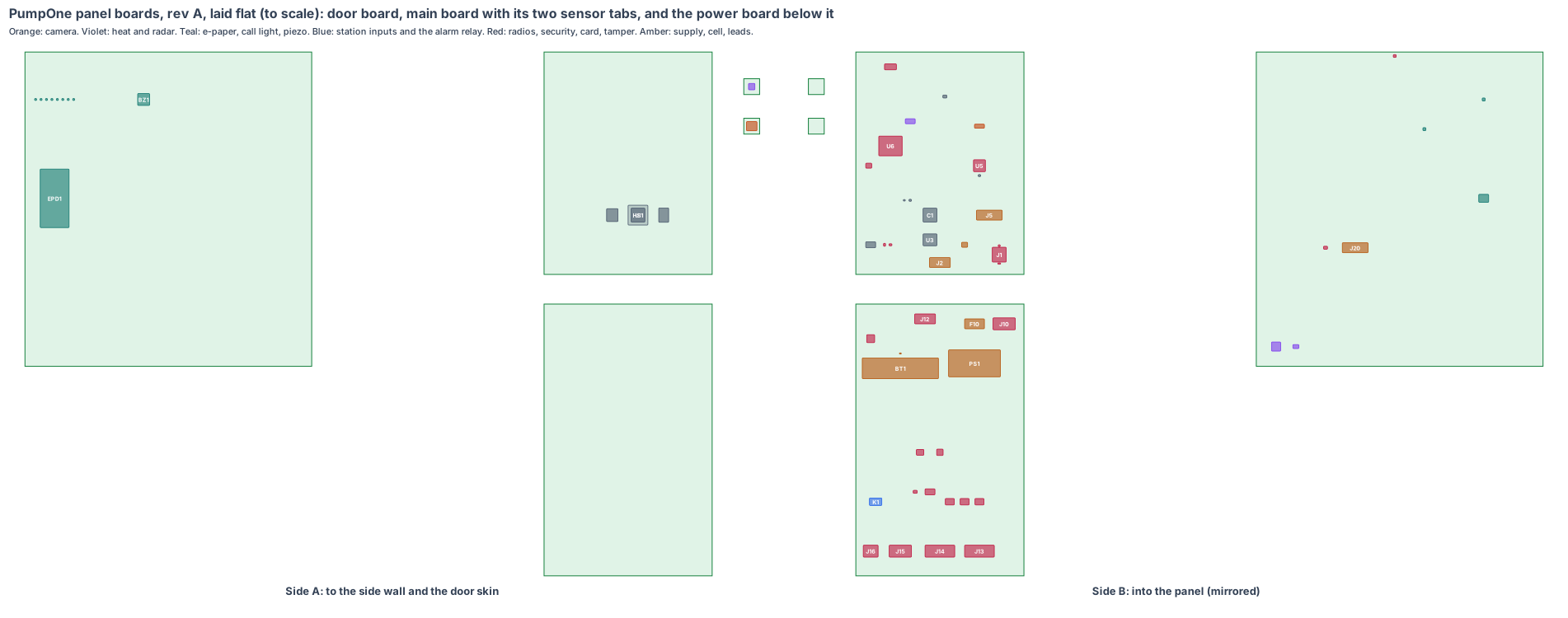
PumpOne: circuit boards of our own
What changed (4 Nov 2026). The rev A bench panel is built from bought boards joined by leads: a Raspberry Pi Zero 2 W, a Camera Module 3 Wide on a ribbon, an HLK-LD2450 radar module, an ADS1115 board, a Walter LTE-M board, an ATECC608 board, an MLX90640 board, a Waveshare e-paper HAT, a NeoPixel stick, a PowerBoost with a LiPo and an IRM-05-5 on flying leads. PumpOne now gets boards of our own, like every IEMI product, with the chips soldered straight on them:
- The chips: the V1 core (Rockchip RV1126B, 2 GB LPDDR4X, 16 GB eMMC, AMPAK AP6256 Wi-Fi/BT module), a bare Sony IMX415 8 MP camera chip under an M12 lens holder (the C1 camera on the board), a TI IWRL6432AOP 60 GHz radar chip with its antennas on the package, a Melexis MLX90640 heat chip, a Quectel BG95-M3 LTE-M module with a soldered eSIM, a TI ADS131M04 ADC with a TI AMC1311 isolated amplifier for the station’s level loop, optocouplers for the float and both pump run calls, a 2.13 in e-paper panel, 8 call-light LEDs, a piezo, a TMAG5273 Hall chip for the door, the security and ID chips.
- The shape: the panel is the same 24 × 20 × 8 in NEMA 4X stainless box, and the plain panel’s breakers, contactors and terminal strip stay on the back plate. So our boards stand on the right side wall, towards the wet well: an 8-layer main board (170 × 225 mm) with the processor and the camera and radar tabs at their windows, and below it a 4-layer power board (170 × 275 mm) with the panel’s 120 V control circuit, the backup cell and every station input on spring-clamp terminals, right beside the pump leads. A 2-layer door board (290 × 318 mm) sits 4 mm inside the door skin with the heat chip looking straight back at the breakers.
- A fix in the same run: the bench LTE-M board and its antenna sat inside the closed stainless box, which stops the signal (new shared lesson: enclosure). A 2-in-1 IP67 puck antenna (LTE-M and 2.4 GHz) now goes through the top wall under the station’s sun shield, its two coax leads soldered to the main board. The camera window grows from a 14 mm disc to a 20 mm square for our M12 lens and the gate call, 34° to the side. Both drawn in the CAD the same day (rev T).
- Made from the shared rules: MEMS clocks, the latched microSD card with our software on every board, conformal coating against hose-down, condensation and hydrogen sulphide from the wet well, a thermistor on the backup cell, the camera and radar 30 mm or more from the processor, every line of sight under 82° from its wall.
The bench panel stays the test rig until the boards arrive. PumpOne only reads and calls: the station’s level controller and alternator keep running the pumps.
1. The shape: three boards, two tabs
| Piece | Size | Layers | Where | What |
|---|---|---|---|---|
| Main board | 170 × 225 mm, 1.6 mm | 8 | standing 20 mm inside the right side wall, top | the V1 core, card, security, LTE-M with eSIM, Wi-Fi/BT, antenna coax pads, lead headers |
| Sensor tabs (2) | 16 × 16 mm, 0.8 mm, on 40 mm flex hinges | 4 | each on its sensor’s axis, the lens or chip just inside its window | IMX415 (station camera, 15° down), IWRL6432AOP (radar, 10° down) |
| Power board | 170 × 275 mm, 1.6 mm | 4 | 8 mm off the right side wall, below the main board | 120 V control-circuit terminal, fuse, IRM-20-5, backup cell and charger, ADC, isolated amplifier, optocouplers, alarm relay, station terminals |
| Door board | 290 × 318 mm, 1.6 mm | 2 | 4 mm inside the door skin | e-paper, call light, piezo (side A); heat chip, tamper Hall chip (side B) |
| Antenna | 2-in-1 IP67 puck, about Ø60 × 22 (est.) | through a Ø17 hole in the top wall, under the sun shield | LTE-M and 2.4 GHz, two RG-178 leads soldered to the main board |
Lead L1 (power board to main board: 5 V on two pairs, cell sense, the ADC’s SPI) is about 0.12 m of 20 AWG with Molex Micro-Fit 3.0 10-pin latched ends. Lead L2 (main board to door board) is about 0.6 m of high-flex 24 AWG in a strain-relieved hinge loop, 14-pin latched ends.
2. What is on the boards
Main board, side A (to the wall): RV1126B (U1) with a 20 × 20 heat block (HS1) to the stainless side wall; LPDDR4X (U2), eMMC (U11); the station camera tab (U200, IMX415 under a 102° M12 lens, 15° down through the 20 × 20 window) and the radar tab (U250, IWRL6432AOP, 10° down behind the 50 × 20 PC window), each held on its axis by a printed bracket.
Main board, side B (into the panel): decoupling field (C1), power (U3), 24 MHz and 32 kHz MEMS oscillators (Y1, Y2), ATECC608B (U8), ID chip (U9), the latched microSD (J1, reached by opening the door), AP6256 (U5), BG95-M3 (U6) with its eSIM (U6S), the antenna coax pads (PD2), camera and radar supplies (U21, U24), ESD array (U25), eFuse (U42), lead headers (J2, J5), factory pads (TP1).
Power board, side B (into the panel): spring-clamp terminal for the panel’s 120 V control circuit (J10), fuse and varistor (F10), IRM-20-5 (PS1), the 18650 holder and cell (BT1) with its thermistor (RT1), the charger (U50), lead header (J12); at the bottom, beside the pump leads and the terminal strip: the ADS131M04 ADC (U51), the AMC1311 isolated amplifier across a 100 Ω shunt in the level loop (U53), three optocouplers for the pump 1 and pump 2 run calls and the high float (U54–U56), current-clamp burdens and filters (U57), input surge guard (U58), the alarm relay (K1), and spring-clamp terminals for the current clamps (J13), the level loop and float (J14), the run calls (J15) and the alarm contact (J16).
Door board, side A (to the door): the e-paper panel (EPD1) in its 26 × 52 window, 8 call-light LEDs (D1–D8) behind the 46 × 6 slot, the piezo (BZ1) behind the tone holes. Side B: the MLX90640 heat chip (U240) looking straight back at both breakers, both contactors and overloads and the terminal strip, its supply (U23), the TMAG5273 Hall chip (U7) at the top edge under the magnet boss, the e-paper booster and FPC pads (U61), LED level shifter (U62), piezo driver (U63), lead header (J20) and ESD array (U64).
3. Every connection, checked
| Link | How | Checked against |
|---|---|---|
| Camera chip to RV1126B | 4-lane MIPI CSI-2 over the tab hinge | IMX415 data sheet: 891 Mbps per lane; at 5 fps it uses 0.41 Gbps of 3.56 |
| Radar chip | SPI and a frame interrupt over the tab hinge | TI IWRL6432AOP data sheet |
| Heat chip, Hall chip | I²C at 3.3 V over lead L2 at 100 kHz | Melexis MLX90640, TI TMAG5273 data sheets |
| E-paper | SPI, busy and reset over L2; the panel’s FPC hot-bar soldered | Good Display GDEY0213B74 data sheet |
| Station inputs | ADS131M04 on SPI over L1 at 1 MHz; the level loop through the AMC1311; run calls and float through optocouplers | TI ADS131M04 and AMC1311 data sheets |
| LTE-M | USB 2.0 and UART on the main board; eSIM soldered; coax to the puck | Quectel BG95 hardware design |
| Wi-Fi/BT | SDIO and UART on the main board; coax to the puck | AMPAK AP6256 (RV1126B SDK default) |
| Power in | the panel’s 120 V control circuit, fused, into the class II IRM-20-5; 5 V on L1 into an eFuse at 3.5 A; L1 drops 0.008 V at 2 A | Mean Well IRM-20 data sheet |
| Alarm | dry relay contact on a spring-clamp terminal to the panel’s own alarm light or autodialer | Omron G5V-1 data sheet |
| Card | SD bus to the RV1126B, latched socket | Amphenol 101-00660 family drawing |
Every mating pair is checked against the makers’ documents, never “same as” another board.
4. Heat
About 1.5 W from the RV1126B goes through the heat block into the shaded stainless side wall (8 K/W est.), so the chip sits near 67 °C with the wall at 55 °C on a hot day. The camera and radar chips are 123 mm or more from the processor.
5. Power budget (est.)
| State | Draw |
|---|---|
| Watching: radar 10 Hz, heat chip 1 Hz while a pump runs, a camera frame every 10 s, ADC at 4 kHz, LTE-M idle | 3.2 W |
| A call: the person model, light and tone, LTE-M callout, the cell charging at 1 A | up to 7.5 W, 38 % of the 20 W supply |
| Power lost: RV1126B asleep, BG95-M3 sends the call and a level report every 5 min | 0.35 W, about 19 h on an aged, cold cell |
6. Factory test (every board, every time)
Spring-pin fixture on TP1 and the door and power boards’ pads: 5 V in, the eFuse trip at 3.5 A, every rail, boot from the card, a frame of a test chart from the camera, a corner reflector seen by the radar, a hot plate seen by the heat chip, a test current through each clamp input, a 4 to 20 mA source on the level input, 120 V on each run-call input, the float input, the relay, the e-paper and all 8 LEDs, the piezo, the Hall chip with a magnet, the security chip’s key, the LTE-M and BLE links on a test puck.
7. Who makes what
One maker makes the main board with its two tabs, the power board and the door board, assembles them (turnkey) and makes leads L1 and L2 to length. We supply the microSD cards with our software and the lens focused at 3 m (est.). The panel builder fits our boards, the windows and the puck antenna into the listed panel. The quote pack is /build/pumpone-quote.
8. Cost per panel, electronics (est.)
| Item | Cost |
|---|---|
| V1 core (RV1126B, 2 GB LPDDR4X, 16 GB eMMC, power, AP6256) | $32 |
| IMX415 camera chip, holder and lens | $14 |
| IWRL6432AOP radar chip | $12 |
| MLX90640 heat chip | $45 |
| BG95-M3 LTE-M and eSIM | $15 |
| 2-in-1 IP67 puck antenna | $25 |
| ADC, isolated amplifier, optocouplers, relay, station terminals | $18 |
| IRM-20-5, mains terminal, fuse, cell, charger | $14 |
| E-paper, LEDs, piezo, Hall, security, ID, socket, passives | $10 |
| Boards (8-layer main with two tabs, 4-layer power, 2-layer door), 1,000 panels | $35 |
| Leads L1 and L2 | $4 |
| Assembly and test | $15 |
| microSD card with our software | $4 |
| Total | about $243 per panel (est.) |
The bench panel’s bought boards cost about $316 at qty 1 (Pi Zero 2 W, camera, radar module, ADC, Walter, MLX90640 board, e-paper, supply, backup and small boards; the current clamps stay), so our boards are about $73 cheaper per panel at 1,000 (est.).
9. Timeline
| Step | When |
|---|---|
| Shape and placement (this page) | done, 4 Nov 2026 |
| Rev T CAD: the boards in the panel CAD, every part checked in 3D; the camera window and antenna hole already drawn | next |
| Schematic, footprints, routing | Dec 2026 – Jan 2027 |
| Rev A boards made and tested | Mar 2027 (est.) |
10. Still to check
- LTE-M from the puck under the steel sun shield at a rural station, against the bench Walter with its antenna inside the box.
- The rev T CAD changes still to draw: the heat block, the tab brackets, the board stand-offs, the magnet boss and the printed shield over the 120 V terminals.
- The level loop’s shunt with the station’s own level controllers (some loops have little spare voltage for 2 V more).
- The 600 mm door lead’s hinge loop over 10,000 door openings.
- Hydrogen sulphide: coating and the stainless windows’ seals after a year at a sewage station.
Sources
- Rockchip RV1126B (Forlinx FET1126Bx-S): https://www.forlinx.net/product/rockchip-rv1126b-som-fet1126b-bj-s-174.html
- Sony IMX415 (8.46 MP, 4-lane MIPI): https://www.sony-semicon.com/en/products/is/security/security.html
- TI IWRL6432AOP: https://www.ti.com/product/IWRL6432AOP
- Melexis MLX90640: https://www.melexis.com/en/product/MLX90640/Far-Infrared-Thermal-Sensor-Array
- Quectel BG95-M3: https://www.quectel.com/product/lpwa-bg95-m3/
- TI ADS131M04: https://www.ti.com/product/ADS131M04
- TI AMC1311: https://www.ti.com/product/AMC1311
- TI TMAG5273: https://www.ti.com/product/TMAG5273
- Good Display GDEY0213B74: https://www.good-display.com/product/391.html
- Mean Well IRM-20: https://www.meanwell.com/Upload/PDF/IRM-20/IRM-20-SPEC.PDF
- Omron G5V-1: https://omronfs.omron.com/en_US/ecb/products/pdf/en-g5v_1.pdf
- Microchip ATECC608B: https://www.microchip.com/en-us/product/atecc608b
- Samsung INR18650-35E: https://www.samsungsdi.com/
- The panel: products/pumpone/cad/pumpone-cad.mjs (rev A, camera window and antenna hole rev T); the boards: products/pumpone/hardware/pcb/pumpone-board.mjs
Design review (4 Nov 2026)
Every board is checked by the same rules (products/_shared/board-rules.mjs), one for each lesson any of our boards has taught us. PumpOne’s boards were made with every rule from the start: 18 pass, 5 fixed, 10 to prove, 0 fail. The full review, with every number and its source, is on the board page. It shows:
- Camera pixels: a 100 mm discharge gauge on the riser (2 m) fills about 108 px against a 40 px need; a person at the gate (3.4 m) about 320 px against 20; the 8 MP chip at 5 fps uses 12 % of its link. The heat chip puts about 2 px on a 25 mm contactor terminal block from the door.
- Every station call in view: the hatch centre and both corners, both riser gauges and the gate; a person at the hatch and at the riser; both breakers, both contactors and the terminal strip, from where each lens or chip really sits.
- The antenna is outside the stainless box (fixed, new lesson: enclosure): a 2-in-1 IP67 puck through the top wall carries both LTE-M and BLE. The rule is now checked on every board, and the boards with radios in metal (DockOne, KitchenOne, PoolOne, RacketOne, ChillOne) each name the window their antenna uses.
- The camera window is a 20 mm square (fixed): sized for our lens rim and the gate call. Drawn in the CAD the same day.
- The station’s own controls stay in charge: the level loop is read through an isolated amplifier across a passive shunt, the run calls through optocouplers, the pump currents with clamps that touch nothing.
- The latched microSD (J1) is fitted, and our software starts from it; updates run only when both pumps are idle and the level is low.
- Fast lines on a solid ground plane (to prove, lesson: planes, from the CricketOne test-board layout of 4 Nov 2026): RV1126B memory; 1 camera MIPI link (100 Ω pairs); USB (90 Ω); antenna feed (50 Ω, keep-out on every layer); card lines (length-matched, no vias under the socket). Ground on the layer next to the parts (inner layer 1, supply on inner layer 2; the whole bottom of a 2-layer section), one via beside each ground and supply pad and none in pads, no copper or vias in the antenna keep-out on any layer or under the card socket, the impedance lines routed first with a test coupon. The quote asks for it; the routed board’s design rule check proves it.
- To prove on rev A: the AI time, the power-cut run on the cell, LTE-M under the sun shield, the tab brackets, the 120 V creepage, the tamper magnet, the leads and the boards in the rev T CAD.
The request for quote is /build/pumpone-quote.
New shared rule (4 Nov 2026, from the CricketOne test-board circuit): the Wi-Fi module’s own clock. Drawing CricketOne’s circuit pin by pin found that the AP6256 Wi-Fi/Bluetooth module runs from a 37.4 MHz reference clock, which our board notes had as 26 MHz or left out. Every board with an AP6256 is now checked for a 37.4 MHz clock beside it (MEMS where the product takes knocks). On this board the AP6256 had no clock of its own on the board; Y3, a 37.4 MHz MEMS oscillator, now sits next to it on side B. The review shows it under Radio (lesson: wificlock).